Dislocation
A dislocation is a line defect in a crystal: a line along which the atoms are out of register, marking the edge of a region that has slipped by one atomic spacing. The size and direction of that slip is the Burgers vector. Dislocations are kept out of silicon wafers but are common in GaN and SiC, where they limit device yield and reliability.
Also called: line defect, edge dislocation, screw dislocation, threading dislocation
Diagram
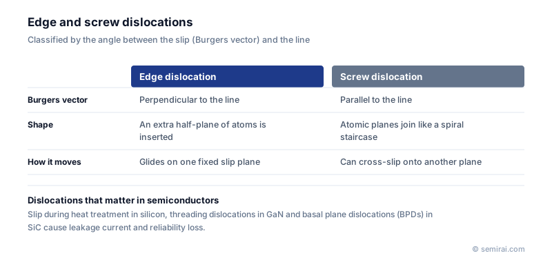
Edge, screw and mixed dislocations
In an edge dislocation the Burgers vector is perpendicular to the dislocation line, as if an extra half-plane of atoms had been pushed into the crystal. In a screw dislocation it is parallel, and the atomic planes wrap around the line like a spiral staircase. Most real dislocations are mixed. A dislocation cannot simply end inside a crystal; it terminates at a surface, meets other dislocations or closes into a loop.
Plastic deformation happens when dislocations glide. Metals bend easily because their dislocations move at room temperature. In silicon the covalent bonds hold them almost still at room temperature, but at processing temperatures they glide on {111} planes and multiply under stress.
Why dislocations harm silicon devices
The distorted bonds along a dislocation create energy levels in the band gap. A dislocation crossing a pn junction becomes a path for leakage current, and metal impurities that collect and precipitate on it can cause local shorts. Silicon ingots are therefore grown dislocation-free. In Czochralski growth, dislocations created when the seed touches the melt are eliminated by necking: the crystal is first pulled to a thin neck a few millimetres across so the dislocations grow out to the surface.
Dislocations can still be introduced later. Uneven heating in a furnace or rapid thermal anneal creates thermal stress, and dislocations called slip run in from the wafer edge or support points. Ramp rates, boat and susceptor design all aim to prevent it.
Dislocations in heteroepitaxy, GaN and SiC
When a film with a different lattice constant grows beyond a critical thickness, misfit dislocations form at the interface, and some turn upward as threading dislocations that reach the surface. GaN grown on silicon or sapphire typically contains around 10⁸–10⁹ threading dislocations per cm², so buffer-layer design is central to GaN devices.
In SiC, basal plane dislocations (BPDs) are the main concern. Under forward current in a bipolar or body-diode mode, recombination energy lets a BPD expand into a stacking fault, raising the on-state voltage over time (bipolar degradation). Epitaxial growth is tuned to convert BPDs into harmless threading edge dislocations near the substrate interface.
Japanese companies involved
- Rigaku makes X-ray topography and diffraction systems used to map dislocations in silicon and SiC wafers.
- Shin-Etsu Chemical and SUMCO supply dislocation-free silicon wafers, and Resonac supplies SiC epitaxial wafers in which reducing BPDs is a key quality target.
- Shin-Etsu Chemical · Silicon wafers, photoresists and photomask blanks
- SUMCO · Silicon wafers
- Resonac · CMP slurries, packaging materials and SiC epitaxial wafers
- Rigaku · X-ray metrology and thermal analysis
FAQ
How are dislocations observed?
Selective chemical etching turns each dislocation that reaches the surface into a pit that can be counted under a microscope; for SiC, molten KOH is commonly used. X-ray topography maps dislocations across a whole wafer without damaging it, and transmission electron microscopy shows individual dislocations at atomic scale.
Why do GaN LEDs work despite so many dislocations?
In InGaN quantum wells, carriers are widely thought to be localised by small fluctuations in indium content before they reach a dislocation, so light emission is less sensitive to dislocations than in other materials. For high-voltage GaN transistors and lasers, however, dislocations still increase leakage and shorten lifetime.
What is the difference between a dislocation and slip?
Slip is the shear of one part of a crystal relative to another along a plane, and dislocations are the mechanism that carries it. In wafer processing, 'slip' refers to bands of dislocations introduced by thermal stress, visible as lines on the wafer surface.
Related pages
- Crystal Defect (Lattice Defect)
- SiC Wafer (Silicon Carbide Substrate)
- Epitaxial Wafer (Epi Wafer)
- GaN-on-Silicon (GaN-on-Si)
- Leakage Current
- PVT (Physical Vapour Transport) Method
- Czochralski Process (CZ Method)
- Lattice Constant
- Crystal growth furnaces
- Daiichi Kiden Round-Chamber Crystal Puller (CZ Method)
- Daiichi Kiden S278 / S380
- Ferrotec FT-CZ1200SE/1400SE
Sources
Last updated: November 13, 2026