Wurtzite Structure
The wurtzite structure is a hexagonal crystal structure in which two kinds of atoms alternate, each forming a hexagonal close-packed framework. Every atom is tetrahedrally surrounded by four atoms of the other kind, as in zincblende, but the atomic layers stack in a two-layer ABAB sequence. It is named after the mineral wurtzite, a form of zinc sulphide.
Also called: wurtzite-type structure
Diagram
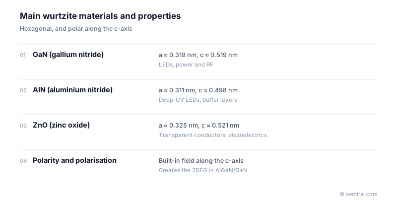
Materials and lattice constants
Many nitride and oxide semiconductors used in blue LEDs and in power and RF devices have this structure, including GaN, AlN, InN and ZnO. Because the crystal is hexagonal, its size is described by two lattice constants: a in the basal plane and c along the c-axis. For GaN, a is about 0.319 nm and c about 0.519 nm.
Films are normally grown along the c-axis, on the so-called c-plane. Sapphire, SiC, silicon and native GaN wafers are all used as substrates, each with a different lattice mismatch.
Polarity and polarisation
The defining feature of wurtzite is polarity along the c-axis. In GaN the gallium face and the nitrogen face behave differently, and the crystal carries a built-in electrical polarisation, called spontaneous polarisation. When AlGaN is grown on GaN, the difference in spontaneous polarisation plus the piezoelectric polarisation from strain draws electrons to the interface. This forms the two-dimensional electron gas (2DEG) that makes the GaN HEMT work without any intentional doping.
The same fields are a drawback in LEDs. They separate electrons and holes inside the quantum wells and reduce light emission efficiency. Growth on non-polar m-plane and a-plane surfaces is studied to avoid this.
Japanese companies involved
- Sumitomo Electric Industries makes compound semiconductor substrates and GaN devices, products built on wurtzite nitride crystals.
- Sumitomo Electric Industries (compound semiconductors) · SiC epitaxial wafers and GaAs and InP substrates
FAQ
How does wurtzite differ from zincblende?
Both have two kinds of atoms with each atom bonded tetrahedrally to four of the other kind. The difference is the stacking: zincblende is cubic with a three-layer ABC sequence, while wurtzite is hexagonal with a two-layer AB sequence. GaAs is zincblende; GaN is normally wurtzite.
What are the c-plane, m-plane and a-plane of GaN?
They are crystal faces of hexagonal GaN. The c-plane is perpendicular to the c-axis and is polar; most growth uses it. The m-plane and a-plane are parallel to the c-axis, so the polarisation does not appear across the surface, which is why they are studied for more efficient LEDs.
Related pages
- Gallium Nitride (GaN)
- Zincblende Structure
- Aluminium Nitride (AlN)
- Two-Dimensional Electron Gas (2DEG)
- Sapphire Substrate
- Semiconductor materials (wafers and substrates)
- Compound semiconductor wafers
- Sumitomo Electric Industries (compound semiconductors) GaAs and InP substrates
- Sumitomo Electric Industries (compound semiconductors) GaN substrates
- Resonac InP epitaxial wafers
- Shin-Etsu Chemical 300 mm silicon wafers
Sources
Last updated: November 12, 2026