Zincblende Structure
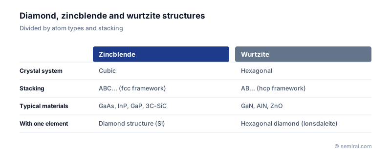
The zincblende structure is a cubic crystal structure with the same atomic arrangement as diamond, except that two kinds of atoms alternate. It is named after the mineral zincblende (sphalerite, ZnS). Each kind of atom forms a face-centred cubic lattice, and every atom is surrounded tetrahedrally by four atoms of the other kind.
Also called: zinc blende structure, sphalerite structure
Diagram
Materials with this structure
The two face-centred cubic lattices are offset from each other by one quarter of the cube's body diagonal. Many III-V compound semiconductors take this form, including GaAs, InP, GaP, InAs and AlAs, as does cubic silicon carbide (3C-SiC).
Because the framework is the same as silicon's, tools such as Miller indices and the same cleavage and orientation conventions carry over directly. That makes it easy to compare GaAs or InP wafers with silicon ones.
Polarity: what changes with two elements
Having two kinds of atoms gives the structure polarity along certain directions. In GaAs, for example, one (111) face ends in gallium atoms and the opposite face ends in arsenic atoms. These faces differ in surface chemistry, etch rate and growth behaviour, so the wafer orientation matters in processing.
When the same pairs of atoms stack in a hexagonal sequence instead, the result is the wurtzite structure. GaN and ZnO normally crystallise as wurtzite, but zincblende forms can be grown under suitable conditions. Understanding the zincblende structure is basic to compound semiconductor substrates and epitaxial growth.
Japanese companies involved
- Sumitomo Electric Industries makes GaAs and InP substrates, both of which have the zincblende structure.
- Sumitomo Electric Industries (compound semiconductors) · SiC epitaxial wafers and GaAs and InP substrates
FAQ
How does the zincblende structure differ from the diamond structure?
The positions of the atoms are identical; only the elements differ. In the diamond structure, as in silicon, all atoms are the same element. In zincblende, two elements such as Ga and As alternate, which gives some crystal faces a polarity that the diamond structure does not have.
Why does GaAs cleave so easily along {110} planes?
The {110} planes contain equal numbers of both atoms, so they are electrically neutral and break cleanly. This natural cleavage is used to form the mirror facets of GaAs and InP laser diodes.
Related pages
- Gallium Arsenide (GaAs)
- Indium Phosphide (InP)
- Wurtzite Structure
- Compound Semiconductor
- II-VI Compound Semiconductor
- Semiconductor materials (wafers and substrates)
- Compound semiconductor wafers
- Sumitomo Electric Industries (compound semiconductors) GaAs and InP substrates
- Sumitomo Electric Industries (compound semiconductors) GaN substrates
- Resonac InP epitaxial wafers
- Shin-Etsu Chemical 300 mm silicon wafers
Sources
Last updated: November 12, 2026