Buffer Layer
A buffer layer is an intermediate layer placed between a substrate and the layer in which the device operates. When two materials with different properties are grown directly on each other, defects, strain and cracks appear; the buffer absorbs those differences so that the active layer grows with good quality.
Also called: transition layer, strain relief layer, field stop layer (IGBT)
Diagram
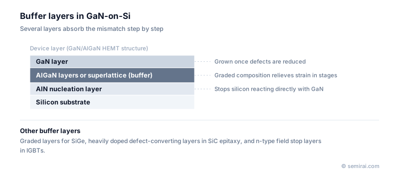
Buffer layers in GaN-on-Si
Gallium nitride grown on silicon is the best-known case. GaN and silicon differ strongly in lattice constant and in thermal expansion. Grown directly, GaN would be full of dislocations, and the wafer would crack or bow badly as it cools after growth.
The usual solution is a stack. A thin aluminium nitride (AlN) nucleation layer comes first, which also stops gallium from reacting with the silicon. On top come AlGaN layers whose aluminium content steps down gradually, or superlattices made of many thin alternating layers. These relieve the strain in stages before the device-quality GaN is grown. A similar idea, a buffer whose composition changes gradually, is used when silicon-germanium is grown on silicon.
Other meanings: SiC epitaxy and IGBTs
In silicon carbide epitaxy, basal plane dislocations can run up from the substrate into the device layer. When current flows in a bipolar mode, these can grow into stacking faults and degrade the device, an effect known as bipolar degradation. A heavily doped buffer layer converts many of these dislocations into a less harmful type and keeps carriers from reaching the remaining ones.
In IGBTs the term has another meaning: a heavily doped n-type layer that stops the electric field from spreading further, also called a field stop layer. It allows a thinner drift region for the same blocking voltage.
Japanese companies involved
- Sumitomo Electric Industries makes SiC epitaxial wafers and compound semiconductor substrates, products in which buffer layer design is part of the epitaxial structure.
- Taiyo Nippon Sanso makes MOCVD equipment of the kind used to grow nitride layer stacks, alongside its specialty gases.
- Taiyo Nippon Sanso · Specialty gases, gas supply systems and MOCVD equipment
- Sumitomo Electric Industries (compound semiconductors) · SiC epitaxial wafers and GaAs and InP substrates
FAQ
Why does GaN-on-Si need such a thick buffer?
The buffer has two jobs at once. It must balance the tensile stress that builds up on cooling, so the wafer stays flat and crack-free, and it must insulate the device from the conductive silicon substrate for high-voltage operation. Meeting both usually takes a buffer several micrometres thick.
Is the buffer layer part of the working device?
Usually not directly. Current flows in the layers above it, such as the AlGaN/GaN channel of a HEMT. But leakage, trapping and breakdown often originate in the buffer, so its quality strongly affects reliability.
Related pages
- GaN-on-Silicon (GaN-on-Si)
- Epitaxy (Epitaxial Growth)
- Lattice Constant
- Aluminium Nitride (AlN)
- SiC Wafer (Silicon Carbide Substrate)
- IGBT (Insulated Gate Bipolar Transistor)
- Heterojunction
- Epitaxial Wafer (Epi Wafer)
- Epitaxial growth equipment
- MOCVD equipment
- Taiyo Nippon Sanso BMC301
- Taiyo Nippon Sanso FR2000-OX
- Taiyo Nippon Sanso SR-4000HT
- Taiyo Nippon Sanso UR25K
Sources
Last updated: November 13, 2026