Gallium Nitride (GaN)
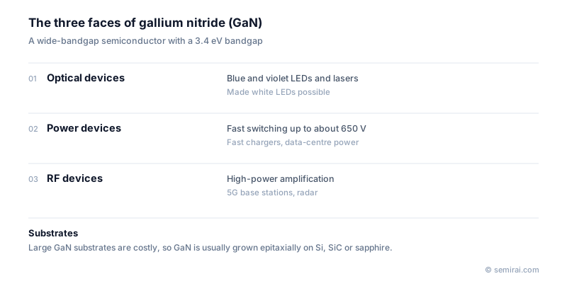
Gallium nitride (GaN) is a III-V compound semiconductor made of gallium and nitrogen, with a wide bandgap of about 3.4 eV. Its high breakdown field and fast electrons make it a key material for three kinds of device: blue and violet light emitters, efficient power transistors, and high-frequency, high-power amplifiers.
Also called: GaN
Diagram
Light emitters
Light-emitting diodes and laser diodes made from InGaN quantum wells on GaN emit blue, violet and green light. Combining a blue LED with a yellow phosphor gives white light, which made LED lighting and LED backlights possible. The work of Isamu Akasaki, Hiroshi Amano and Shuji Nakamura on efficient blue LEDs received the 2014 Nobel Prize in Physics; Nakamura carried out his work at Nichia.
Power and RF transistors
Most GaN transistors are HEMTs (high-electron-mobility transistors). At the interface between AlGaN and GaN, a two-dimensional electron gas forms without doping, giving high electron mobility and high carrier density. Compared with silicon MOSFETs, GaN power transistors have much lower switching losses and can switch at higher frequencies, so the inductors and capacitors around them can be smaller. They are used in compact USB chargers, server power supplies and other converters, mainly at voltages of 650 V and below.
RF GaN HEMTs, usually built on SiC substrates for their good heat conduction, deliver high output power at high frequencies. They are used in power amplifiers for mobile base stations, radar and satellite communications.
Substrates and growth
Large, low-cost GaN substrates are hard to produce, so GaN layers are usually grown by MOCVD on silicon, SiC or sapphire. GaN-on-silicon can use large silicon wafers and existing fabs, which lowers cost for power devices. GaN-on-SiC is preferred for RF, and sapphire is common for LEDs. The large lattice and thermal mismatch with silicon requires buffer layers to control dislocations and wafer bow.
Japanese companies involved
- Nichia makes GaN-based LEDs and laser diodes.
- Sumitomo Electric Industries and Mitsubishi Electric make GaN HEMTs for RF amplifiers.
- Sumitomo Electric Industries (compound semiconductors) · SiC epitaxial wafers and GaAs and InP substrates
- Mitsubishi Electric (power devices) · IGBT and SiC power modules, RF and optical devices
- Nichia · LEDs and laser diodes
FAQ
How does GaN compare with SiC for power devices?
Both are wide-bandgap materials. GaN switches faster and suits compact converters up to roughly 650 V. SiC handles higher voltages and currents and conducts heat better, so it dominates in electric-vehicle traction inverters and other high-voltage systems above that range.
Why are most GaN power transistors normally on?
The two-dimensional electron gas forms by itself at the AlGaN/GaN interface, so a basic HEMT conducts with zero gate voltage. Power circuits need devices that stay off when the gate is not driven, so manufacturers use p-GaN gates, recessed gates or a cascode with a silicon MOSFET to make them normally off.
What is a GaN charger?
It is a power adapter whose main switching transistors are GaN instead of silicon. Because GaN switches efficiently at higher frequencies, the transformer and other passive parts can be smaller, giving a lighter charger for the same output power.
Comparisons
Related pages
Sources
Last updated: November 2, 2026