Sapphire Substrate
A sapphire substrate is a wafer cut from single-crystal aluminium oxide (α-Al₂O₃). It has been the most widely used growth substrate for gallium nitride (GaN) blue LEDs, and so for white LEDs, because it allowed GaN to be grown in volume at a time when native GaN substrates were expensive and hard to obtain.
Also called: sapphire wafer, PSS (patterned sapphire substrate)
Diagram
How sapphire wafers are made
Large single-crystal boules are grown by methods such as the Kyropoulos method, edge-defined film-fed growth (EFG) or the heat exchanger method. Cylinders are cored out of the boule, sliced with wire saws, then lapped and polished.
Sapphire has a Mohs hardness of 9, so cutting and polishing take a long time and need diamond abrasives. Machining therefore makes up a large part of the wafer cost.
Making GaN work on sapphire
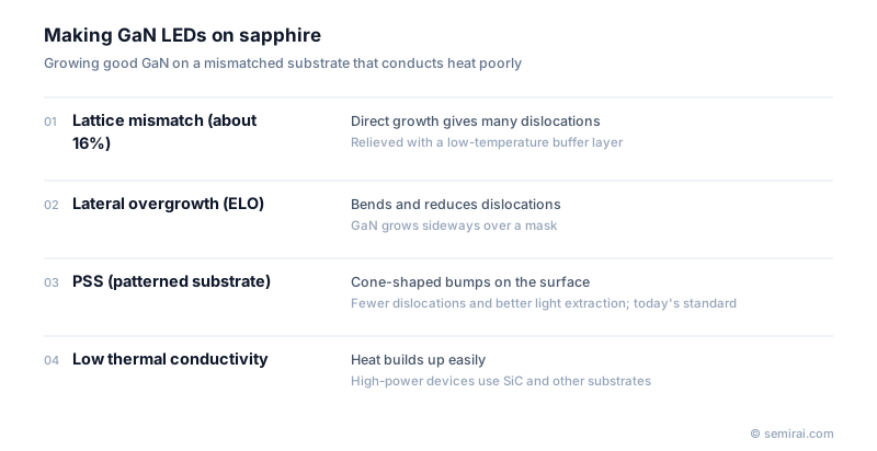
Sapphire is far from an ideal match for GaN. The lattice mismatch is about 16%, the thermal expansion differs, and sapphire conducts heat poorly. The breakthrough was a thin low-temperature buffer layer of AlN or GaN, together with techniques such as epitaxial lateral overgrowth (ELO), which reduced the dislocation density enough for practical LEDs.
Today the standard LED substrate is the patterned sapphire substrate (PSS). Its surface carries an array of cones a few micrometres in size. These bend dislocations sideways so fewer reach the active layer, and they scatter light so more of it escapes the chip.
Sapphire is an electrical insulator, so both electrodes must be taken out from the top of the device in a lateral structure. Its poor heat conduction limits high-power devices, where SiC or GaN substrates are used instead.
Japanese companies involved
- Kyocera makes single-crystal sapphire wafers for LED production.
- Nichia makes GaN-based LEDs and laser diodes and was central to the commercialisation of the blue LED.
FAQ
Is sapphire still used now that GaN-on-Si and GaN substrates exist?
Yes. Each substrate now has its own niche, but for general lighting and display backlight LEDs sapphire remains the main substrate because it is mature and cost-effective. Micro-LED development has also created new demand for it.
Why is a sapphire wafer transparent?
Sapphire has a very wide band gap, so it does not absorb visible light. This lets light emitted downward in an LED pass through the substrate, which is one reason flip-chip LEDs can emit through the sapphire side.
What else is sapphire used for in electronics?
Besides LEDs, sapphire is used for silicon-on-sapphire (SOS) RF circuits, optical windows and wear-resistant covers, because it is hard, transparent and electrically insulating.
Related pages
- Light-Emitting Diode (LED)
- Gallium Nitride (GaN)
- GaN-on-Silicon (GaN-on-Si)
- Laser Slicing / Laser Lift-off
- Compound Semiconductor
- Substrate
- Wurtzite Structure
- Epitaxy (Epitaxial Growth)
- Compound semiconductor substrate equipment (SiC/GaN)
- Compound semiconductor equipment
- Wafer polishing and edge grinding equipment
- Canon ANELVA EC8100
- Daiichi Kiden Solution Growth System
- DISCO DFP8141
- Fujikoshi Machinery LSL-19A
Sources
Last updated: November 13, 2026