Compound Semiconductor
A compound semiconductor is a semiconductor material made by combining two or more elements, such as gallium arsenide (GaAs), gallium nitride (GaN), silicon carbide (SiC) and indium phosphide (InP). Unlike the elemental semiconductors silicon and germanium, these materials can emit light efficiently, move electrons faster or withstand higher voltages.
Also called: III-V semiconductor, wide-bandgap semiconductor
Diagram
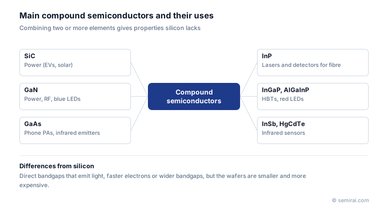
What compound semiconductors can do that silicon cannot
Silicon has an indirect bandgap, so it converts electricity into light very poorly. Many compound semiconductors, including GaAs, InP and GaN, have a direct bandgap and emit light efficiently. This is why LEDs, laser diodes and many photodetectors are made from them: GaN-based LEDs give blue and white light, GaAs-based VCSELs (vertical-cavity surface-emitting lasers) are used for face recognition and short-reach data links, and InP lasers carry long-distance and data-centre optical traffic.
Electron mobility in GaAs and InP is several times that of silicon, which suits low-noise, high-frequency transistors such as the power amplifiers and switches in mobile phones. Wide-bandgap materials, mainly SiC and GaN, tolerate much higher electric fields before breakdown, so power transistors made from them can be thinner, switch faster and lose less energy. SiC is widely used in electric-vehicle inverters, and GaN in compact fast chargers and RF amplifiers for base stations and radar.
How they are made
Device fabrication uses the same basic steps as silicon: lithography, etching, deposition and implantation. The difference lies in the starting material. Compound substrates are smaller and more expensive than silicon wafers, typically 100 mm to 150 mm for GaAs and InP and 150 mm to 200 mm for SiC. GaN is usually grown on another substrate such as silicon, SiC or sapphire.
The active layers are grown by epitaxy, most often MOCVD (metal-organic chemical vapour deposition) or MBE (molecular beam epitaxy), which can stack layers of different composition with atomic-scale control. These stacked heterostructures are the basis of HEMTs, HBTs, quantum-well lasers and LEDs.
Japanese companies involved
- Sumitomo Electric Industries makes GaAs and InP substrates and SiC epitaxial wafers.
- Nichia makes GaN-based LEDs and laser diodes, and Mitsubishi Electric makes SiC power modules as well as RF and optical devices built on compound semiconductors.
- Sumitomo Electric Industries (compound semiconductors) · SiC epitaxial wafers and GaAs and InP substrates
- Nichia · LEDs and laser diodes
- Mitsubishi Electric (power devices) · IGBT and SiC power modules, RF and optical devices
- Tokyo Electron (TEL) · Coat/develop, etch and deposition equipment
FAQ
Is silicon carbide a III-V semiconductor?
No. SiC combines two group IV elements, so it is a IV-IV compound. GaAs, GaN and InP combine a group III element with a group V element and are III-V compounds. Materials such as ZnSe and CdTe are II-VI compounds, and HgCdTe is used for infrared detectors.
Why are compound semiconductors more expensive than silicon?
Their crystals are harder to grow without defects, the wafers are smaller and more fragile, and some raw materials such as indium and gallium are produced in small volumes. Fewer chips fit on each wafer and each wafer costs more, so they are used where their properties are essential.
Related pages
Sources
Last updated: November 13, 2026