Two-Dimensional Electron Gas (2DEG)
A two-dimensional electron gas (2DEG) is a very thin sheet of electrons trapped at an interface, typically between two different semiconductors, where they can move freely only within the plane. They cannot move in the thickness direction, hence two-dimensional. The 2DEG is the current channel of the high electron mobility transistor (HEMT).
Also called: 2DEG
Diagram
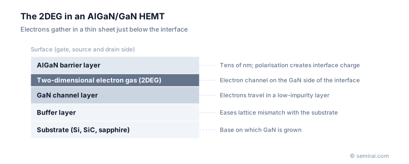
AlGaAs/GaAs and AlGaN/GaN
In the AlGaAs/GaAs system, electrons from donor atoms in the doped AlGaAs layer move into the neighbouring GaAs and collect at the interface. They travel on the GaAs side, away from the donors, so they scatter less and reach very high mobility. This separation of dopants from the channel is called modulation doping. The HEMT based on it was invented at Fujitsu around 1980 by Takashi Mimura.
In AlGaN/GaN, the polarisation of the crystals produces a 2DEG with a sheet density around 10¹³ electrons per cm² even without intentional doping.
Why it matters for devices
High electron density combined with high mobility makes the 2DEG suitable for transistors that operate at high frequency and for power transistors that carry large currents with low resistance. GaN HEMTs are used in mobile base stations and fast chargers.
Because the 2DEG in GaN exists without any gate voltage, a simple GaN HEMT is normally-on: current flows when the gate is at zero volts. Power circuits need normally-off devices for safety, so manufacturers use structures such as p-GaN gates or recessed gates. In physics, two-dimensional electron systems were where the quantum Hall effect was discovered.
Japanese companies involved
- Sumitomo Electric Industries makes GaN HEMTs for radio-frequency amplifiers as well as compound semiconductor substrates.
- ROHM produces GaN HEMTs for power conversion.
- Sumitomo Electric Industries (compound semiconductors) · SiC epitaxial wafers and GaAs and InP substrates
- ROHM · SiC and silicon power devices, analog ICs
FAQ
Why do GaN 2DEGs form without doping?
GaN and AlGaN have built-in spontaneous polarisation because of their crystal structure, and strain in the thin AlGaN layer adds piezoelectric polarisation. The difference in polarisation leaves a fixed positive charge at the interface, and electrons accumulate to balance it.
What substrates are used for GaN HEMTs?
GaN is usually grown on a foreign substrate with a buffer layer to manage the lattice mismatch. Silicon carbide is common for RF devices because it removes heat well, silicon is used for lower-cost power devices, and sapphire is also used.
Related pages
Sources
Last updated: November 2, 2026