Air Gap Dielectric
An air gap dielectric uses air, rather than a solid low-dielectric-constant (low-k) material, as the insulator between metal lines in a chip's interconnect. Air has a relative permittivity (k) of about 1.0, lower than any solid insulator, so air gaps reduce the parasitic capacitance between neighbouring wires, cutting signal delay and dynamic power consumption.
Also called: air gap, airgap interconnect
Diagram
Why air gaps are needed
As interconnect pitch shrinks, adjacent wires come closer and the capacitance between them grows. That capacitance, multiplied by the wire resistance, sets RC delay, and it also adds crosstalk and switching power. Silicon dioxide has k of about 3.9; carbon-doped oxides (SiOC) bring this to roughly 2.5-3.0, and porous ultra-low-k films lower still. Porous films, however, are mechanically weak and easily damaged during processing. Replacing the insulator between the tightest lines with air is the most direct way to go further.
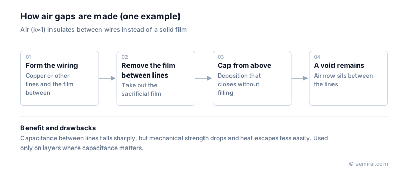
Air gaps are not used everywhere. They weaken the stack mechanically and conduct heat poorly, so they are applied only to the layers where line-to-line capacitance matters most.
How air gaps are made
In a damascene flow, copper lines are formed in a dielectric, the dielectric between selected lines is then etched away, and a cap layer is deposited by a non-conformal process that bridges the gap without filling it. In subtractive or semi-damascene flows, metal lines are etched from a blanket film and the spaces between them are closed off the same way, which makes air gaps easier to form. Highly selective etching and well-controlled capping are the key steps, and cross-sections by electron microscopy are used to check the gap shape.
IBM announced an air-gap interconnect technique in 2007, and Intel used air gaps in selected interconnect layers of its 14nm process.
Japanese companies involved
- Tokyo Electron supplies etch and deposition equipment of the kind used to remove sacrificial dielectrics and cap the gaps.
- Japanese academic and government reviews of beyond-2nm interconnect identify air gaps alongside new metals as a key direction.
- Tokyo Electron (TEL) · Coat/develop, etch and deposition equipment
FAQ
Why not use air gaps in every layer?
Air gaps reduce the mechanical strength of the interconnect stack and conduct heat poorly. Vias landing next to a gap can also break into it. Manufacturers therefore use them only in the tight-pitch layers where capacitance limits performance.
How does an air gap stay empty during later processing?
The cap film is deposited with a method that pinches off at the top of the narrow space before it can fill it, sealing a void underneath. Later layers are built on top of the cap as usual.
Related pages
Sources
Last updated: November 2, 2026