5nm Process (5nm Node)
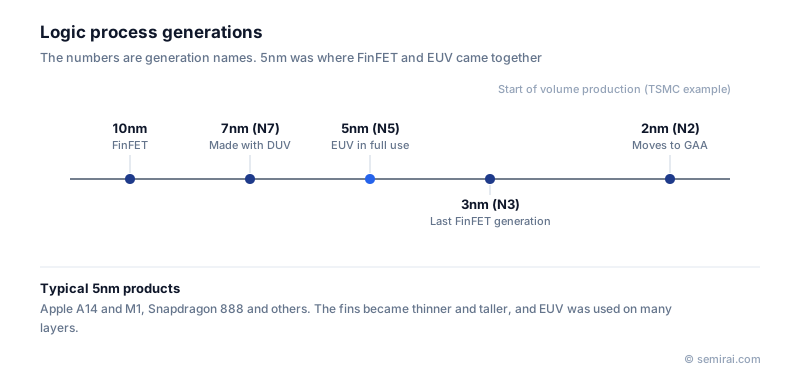
The 5nm process is the generation of logic manufacturing technology that follows the 7nm node. The number is a generation name rather than a physical dimension: no feature on the chip is actually 5 nm wide. TSMC and Samsung both began volume production at this node in 2020, and it became one of the most heavily used advanced nodes for smartphone and computer processors.
Also called: 5 nm node, N5, 5LPE
Diagram
What changed from 7nm
The transistor is still a FinFET, in which the gate wraps the channel on three sides, but the fins are narrower, taller and placed closer together, and the gate and metal pitches are tighter. The biggest change was in lithography. Where the first 7nm processes relied on deep ultraviolet (DUV) immersion lithography with multiple patterning, 5nm used extreme ultraviolet (EUV) lithography on many critical layers, combined with self-aligned double and quadruple patterning (SADP and SAQP) where needed.
TSMC describes its N5 process as offering roughly 1.8 times the logic density of N7, together with either higher speed at the same power or lower power at the same speed. Gains of this kind are the reason a new node is adopted, and are usually summarised as power, performance and area (PPA).
The 5nm family
A node is rarely a single process. TSMC followed N5 with N5P and then the N4 variants (N4, N4P, N4X), which reuse most of the 5nm design rules while adding performance or density. Samsung moved from 5LPE to 5LPP and on to its 4nm processes. Because designs can move between these variants with limited rework, the 5nm family stayed in high-volume production for years, carrying smartphone systems-on-chip (SoCs), PC processors and AI accelerators.
Japanese companies involved
- Tokyo Electron supplies coater/developers used with EUV scanners, as well as etch, deposition and cleaning tools used at 5nm-class fabs.
- Hitachi High-Tech makes CD-SEM systems that measure the critical dimensions of the fine patterns printed at this node.
- Tokyo Electron (TEL) · Coat/develop, etch and deposition equipment
- Hitachi High-Tech · CD-SEM metrology, defect inspection and etch systems
FAQ
Is anything on a 5nm chip actually 5 nm wide?
Not in the sense the name suggests. Node names stopped matching gate length or half-pitch years ago. Real dimensions such as contacted gate pitch and minimum metal pitch are several times larger, so density metrics are more useful than the name when comparing processes.
Is TSMC 5nm the same as Samsung 5nm?
No. Each company chooses its own names, and processes with the same number can differ in density, transistor design and performance. Comparisons should be made with published pitches or density figures rather than the node number alone.
What came after 5nm?
The 3nm generation, which was the last to use FinFETs at TSMC, followed by 2nm, where the industry moved to gate-all-around nanosheet transistors.
Related pages
Sources
Last updated: November 2, 2026