Logic Process
A logic process is the manufacturing technology used to build digital computing chips such as CPUs, GPUs, FPGAs, systems-on-chip (SoCs) and ASICs. Logic here means circuits that carry out Boolean operations such as AND, OR and NOT, built from very large numbers of MOSFETs. Logic processes are tuned for transistor speed, low power and density, in contrast to memory processes, which are tuned for bit cost.
Also called: logic technology, logic node
Diagram
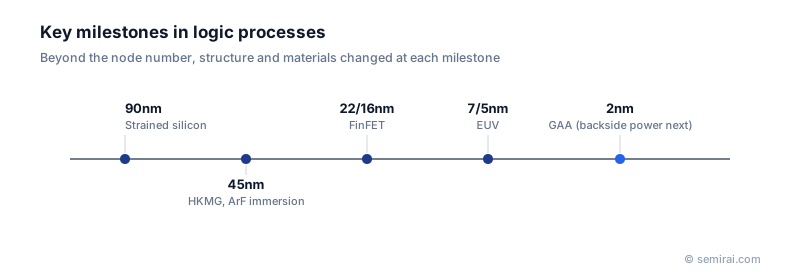
How logic nodes have advanced
Logic processes are released in generations, or nodes, each with a smaller name: 28nm, 22nm, 16/14nm, 10nm, 7nm, 5nm, 3nm and 2nm. The number has long ceased to be a physical dimension, but each step brings more transistors per area, higher speed or lower power.
The real milestones have been changes in structure and materials. Strained silicon raised carrier mobility around the 90nm generation. High-k metal gates (HKMG) replaced silicon dioxide and polysilicon at 45nm. FinFETs arrived at 22/16nm. EUV lithography entered volume production at 7nm and 5nm. At 2nm the transistor changes again to gate-all-around (GAA) nanosheets, and backside power delivery follows.
What a leading-edge logic process contains
A modern logic process combines the transistor (FinFET or nanosheet), the gate stack deposited by atomic layer deposition, more than ten layers of copper and low-k interconnect, and increasingly advanced packaging such as TSMC's CoWoS and SoIC or Intel's Foveros. Hundreds of process steps and dozens of lithography layers are needed.
At the leading edge, TSMC, Samsung Foundry and Intel Foundry compete. TSMC's N3 has been used in Apple's A17 Pro and M3 processors, Samsung's SF3 uses its MBCFET version of GAA, and Intel 18A combines RibbonFET transistors with PowerVia backside power.
Japanese companies involved
- Rapidus is developing a 2nm logic process at its pilot line in Chitose, Hokkaido, aiming to be Japan's first leading-edge logic foundry.
- Tokyo Electron (coater/developers, etch, deposition) and SCREEN Holdings (wafer cleaning) supply process equipment used throughout logic fabs.
- Rapidus · Leading-edge logic foundry (2 nm, in development)
- Tokyo Electron (TEL) · Coat/develop, etch and deposition equipment
- SCREEN Holdings · Wafer cleaning, coat/develop and inspection equipment
FAQ
What is the difference between a logic process and a memory process?
A logic process aims for fast transistors and many interconnect layers to wire up varied circuits. A memory process repeats one cell billions of times and aims for the lowest cost per bit, so its hardest steps are the DRAM capacitor or the deep holes of 3D NAND.
Do analog chips use logic processes?
Many analog and power chips use mature or specialised processes, such as BCD processes with high-voltage devices, because shrinking transistors brings little benefit to analog performance.
Related pages
Sources
Last updated: November 2, 2026