Through-Silicon Via (TSV)
A through-silicon via (TSV) is a vertical electrical connection that passes completely through a silicon wafer or die, made by etching a deep hole, insulating it and filling it with metal, usually copper. TSVs let stacked dies, or a die and a silicon interposer, connect directly through the silicon with thousands of short links instead of wire bonds around the edge.
Also called: TSV, through-silicon electrode
Diagram
Why TSVs matter
Wire bonds run from pads at the edge of a die and are millimetres long. A TSV is only as long as the thinned die is thick, typically tens of micrometres, and can be placed anywhere in the die area on a pitch of tens of micrometres or less. A single die can therefore carry thousands of connections, with lower resistance, capacitance and inductance per link. That combination of many short, parallel connections is what gives stacked memory its bandwidth at reasonable power.
The best-known use is HBM (high bandwidth memory), where several DRAM dies and a base die are stacked and joined by TSVs, and the stack sits beside a processor on a silicon interposer that itself uses TSVs to reach the package substrate. TSVs are also used in some CMOS image sensors, 3D ICs that stack logic and memory, and MEMS.
How a TSV is made
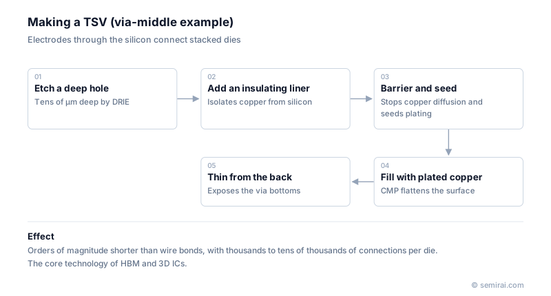
The hole is etched by deep reactive ion etching (DRIE), which alternates etch and sidewall passivation to cut straight, deep holes, usually with depth-to-diameter ratios of about 5:1 to 20:1. An insulating liner of silicon oxide or nitride separates the copper from the silicon. A barrier such as Ta or TaN stops copper diffusing, a copper seed layer is deposited, and the hole is filled by electroplating without voids. Chemical mechanical polishing (CMP) removes the excess copper from the surface.
The wafer is then bonded face-down to a temporary carrier, thinned from the back until the via tips are exposed, and given backside insulation and pads or bumps. Depending on when the via is formed, the flow is called via-first (before transistors), via-middle (after transistors, before the upper wiring) or via-last (from the back after wafer processing). Via-middle is the common choice for memory and logic.
Engineering challenges
Copper and silicon expand at different rates, so a TSV creates stress that can shift the behaviour of nearby transistors; designers keep a keep-out zone around each via. Copper can also protrude from the via after annealing, damaging the layers above. Thinned wafers warp and break easily, and every via in a stack must work, so testing dies before stacking is essential.
Japanese companies involved
- Tokyo Electron supplies etch, deposition, and wafer bonding and debonding systems used in TSV and 3D-stacking process flows.
- DISCO's grinders and dicing saws are used to thin wafers to expose TSVs and to separate stacked dies.
- DISCO · Dicing, grinding and polishing equipment
- Tokyo Electron (TEL) · Coat/develop, etch and deposition equipment
FAQ
What is the difference between a TSV and a micro-bump?
A TSV carries signals vertically through a die. A micro-bump is a small solder or copper joint on the die surface that connects one die's TSV pads to the next die. In a stack, signals pass through a TSV, then a micro-bump or hybrid bond, then the next TSV.
Do all advanced packages use TSVs?
No. Fan-out packages and silicon bridges embedded in substrates connect dies side by side without vias through the active dies. TSVs are needed when dies are stacked vertically, or when a silicon interposer must pass signals from its top to the substrate below.
Is TSV used in 3D NAND?
Not to build the memory array. 3D NAND stacks cells within one die in a single process. Separate NAND dies in a package are usually connected by wire bonds, although TSV-stacked NAND has been demonstrated for high-performance uses.
Comparisons
Related pages
- Advanced Packaging
- HBM (High Bandwidth Memory)
- Copper Interconnect (Damascene Process)
- CMP (Chemical Mechanical Polishing)
- Backgrinder (Back Grinding Equipment)
- Wafer Thinning
- Temporary Bonding and Debonding (TBDB)
- Bosch Process
- TSV formation equipment
- Ebara UFP600AS
- Lasertec BGM300
- Lasertec VIANCA series
- SAMCO RIE-800BCT
Sources
Last updated: November 13, 2026