CSP (Chip Scale Package)
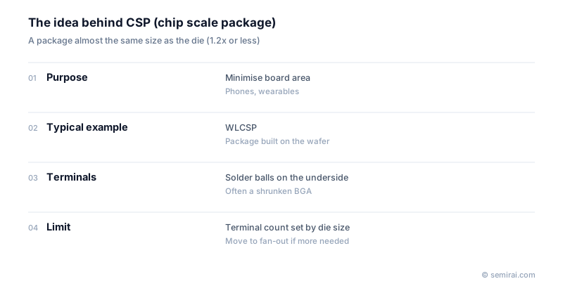
A CSP (chip scale package, also called chip size package) is a package whose outline is only slightly larger than the die inside it, commonly defined as no more than 1.2 times the die size. Keeping the package almost as small as the chip minimises board area and height, which is why CSPs are widely used in smartphones, wearables and other compact devices.
Also called: chip size package, WLCSP
Diagram
Forms of CSP
CSP is a definition based on size, not a single structure. In a wafer-level CSP (WLCSP), redistribution wiring and solder balls are formed on the wafer itself, and the wafer is then diced, so the package is exactly the size of the die. This is a fan-in package: all terminals must fit within the die area.
Other CSPs mount the die on a small substrate or tape, using either wire bonds or flip-chip bumps, with solder balls underneath. These are essentially miniature BGAs. Lead-frame-based packages trimmed close to the die size have also been called CSPs.
Where CSP fits
Compared with leaded packages such as QFP and with standard BGAs, a CSP removes most of the margin around the die. This suits chips with modest pin counts, such as power management ICs, sensors, RF devices and small controllers in mobile products.
When a chip needs more terminals than its own area can hold at a usable ball pitch, a fan-in CSP no longer works. Fan-out wafer-level packaging then extends the wiring beyond the die edge, and larger devices move to flip-chip BGA packages.
Japanese companies involved
- IBIDEN · IC package substrates (FC-BGA)
FAQ
How is a CSP different from a BGA?
BGA describes the terminal format: solder balls in a grid on the bottom. CSP describes the size: a package close to the die size. Many CSPs use solder balls and are therefore also BGAs, so the two terms overlap rather than exclude each other.
What is a WLCSP?
A wafer-level chip scale package, in which the redistribution layer and solder balls are formed on the whole wafer before dicing. No separate assembly is needed for each chip, so the package is the same size as the die and low in cost.
What are the drawbacks of CSPs?
The small size limits the area for heat to escape, and the difference in thermal expansion between the die and the board concentrates stress on the solder joints. The number of terminals is also limited by the die area.
Related pages
Sources
Last updated: November 2, 2026