BGA (Ball Grid Array)
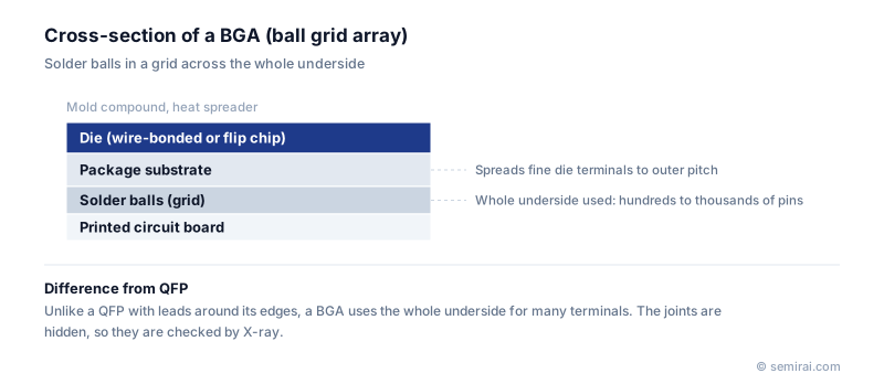
A BGA (ball grid array) is a semiconductor package whose external terminals are solder balls arranged in a grid across its underside. Because the whole bottom surface is used, a BGA offers far more connections than a package with leads only around its edges, from a few hundred to several thousand.
Also called: ball grid array, FC-BGA, PBGA
Diagram
Types of BGA
BGAs are classified mainly by their substrate and by how the die is connected. A plastic BGA (PBGA) uses an organic laminate, usually BT resin, with a wire-bonded die and mold cap. Ceramic BGAs use a ceramic body for higher reliability. In a flip-chip BGA (FC-BGA), the die is bumped and joined face down to a build-up substrate with ABF insulating layers, and a lid or heat spreader is often added.
FC-BGA is the standard package for CPUs, GPUs, FPGAs and network processors. Even advanced 2.5D packages, where several dies sit on an interposer, are normally mounted on a large FC-BGA substrate that provides the final connection to the motherboard.
Mounting and inspection
During board assembly, the balls melt in a reflow oven and surface tension pulls the package into alignment with its pads, so BGAs are tolerant of small placement errors. There are no fragile leads to bend, which helps assembly yield.
The joints, however, are hidden under the package. They are checked by X-ray inspection, and failures are hard to rework. The difference in thermal expansion between the package and the board stresses the outer balls during temperature cycling, so large BGAs may use board-level underfill, careful pad design or corner reinforcement. Package warpage during reflow can cause open joints and must be controlled.
Japanese companies involved
- IBIDEN, Shinko Electric Industries and Kyocera make the substrates used in FC-BGA and other BGA packages, and Senju Metal Industry and Nippon Micrometal supply solder balls.
- Shinko Electric Industries · FC-BGA package substrates and lead frames
- Senju Metal Industry · Solder, flux and solder balls
- Nippon Micrometal · Bonding wire and micro balls
- IBIDEN · IC package substrates (FC-BGA)
- Kyocera · Package substrates and ceramic components
FAQ
How is a BGA different from a QFP?
A quad flat package (QFP) has gull-wing leads around its four sides, so its pin count is limited by the perimeter and fine-pitch leads are easy to bend. A BGA uses the whole underside, so it can carry many more terminals in a smaller area.
What pitch do BGA balls use?
Board-level BGAs commonly use ball pitches from about 1.27 mm down to around 0.4 mm. Finer pitch saves area but needs finer circuit board wiring and more careful assembly.
Related pages
Sources
Last updated: November 2, 2026