Flip Chip
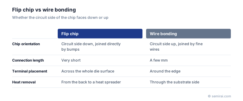
Flip chip is an interconnection method in which a semiconductor die is turned over, with its circuit side facing down, and joined directly to a substrate through small conductive bumps formed on its pads. It replaces the bond wires of conventional packages with very short vertical connections.
Also called: flip-chip bonding, C4, controlled collapse chip connection
Diagram
Why designers choose flip chip
Bond wires are typically a few millimetres long, while a bump is only tens of micrometres high. The shorter path cuts inductance and resistance, so signals switch faster and power is delivered more cleanly. Bumps can also be placed across the whole area of the die rather than only along its edges, which allows hundreds to tens of thousands of connections.
Heat is another advantage. With the active side facing down, the back of the die faces up and can be attached directly to a heat spreader or lid. These properties make flip chip the standard for CPUs, GPUs, network chips and other large, fast devices, usually in a flip-chip ball grid array (FC-BGA) package.
Bumps, bonding and underfill
Early flip chip used tin-lead solder bumps that melt and collapse slightly during reflow; IBM's name for this, controlled collapse chip connection (C4), is still used. Today lead-free tin-silver solder bumps and copper pillars topped with a small solder cap are common. Copper pillars allow finer pitch because they do not spread as much when melted. Gold stud bumps are used in some smaller devices.
Bumps are joined by mass reflow or, at fine pitch, by thermocompression bonding (TCB), which heats and presses one die at a time. Afterwards the gap between die and substrate is filled with underfill resin. Without it, the difference in thermal expansion between silicon and the organic substrate would crack the solder joints during temperature cycling.
Japanese companies involved
- Toray Engineering and Shinkawa (Yamaha Robotics) make flip-chip bonders, and Namics and Resonac supply the underfill materials used after bonding.
- IBIDEN and Shinko Electric Industries make FC-BGA substrates on which flip-chip processors are mounted.
- Toray Engineering · Flip-chip bonders, die bonders and visual inspection systems
- Shinkawa (Yamaha Robotics) · Wire bonders and die bonders
- Namics · Underfill and die attach materials
- Resonac · CMP slurries, packaging materials and SiC epitaxial wafers
- IBIDEN · IC package substrates (FC-BGA)
- Shinko Electric Industries · FC-BGA package substrates and lead frames
FAQ
Is flip chip more expensive than wire bonding?
Usually yes. Bumping the wafer, a finer substrate and underfill all add cost, so wire bonding remains the cheaper choice for chips with modest pin counts and speed. Flip chip pays off when many connections or high speed are needed.
How is flip chip related to hybrid bonding?
Both join a die face down. Flip chip uses solder bumps at pitches of roughly 40 µm and above, while hybrid bonding removes the solder and bonds copper pads directly, reaching pitches of a few micrometres for 3D stacking.
Comparisons
Related pages
Sources
Last updated: November 2, 2026