Advanced Packaging
Advanced packaging is the umbrella term for back-end technologies that integrate several dies, or a die and memory, in one package with far denser connections than a wire-bonded or simple flip-chip package. It lets designers reach performance, bandwidth and cost that a single chip cannot, and it underpins today's AI processors.
Also called: heterogeneous integration, 2.5D/3D packaging
Diagram
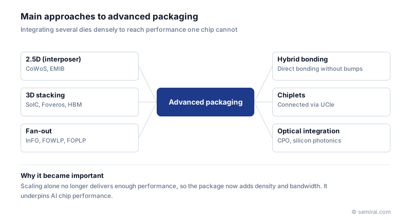
The main approaches
In 2.5D packaging, dies sit side by side on a silicon interposer or a fine-line redistribution layer (RDL) that carries thousands of short connections between them. TSMC's CoWoS and Intel's EMIB, which uses a small silicon bridge embedded in the substrate, are the best-known examples. In 3D packaging, dies are stacked vertically and connected through through-silicon vias (TSVs), as in high bandwidth memory (HBM), TSMC's SoIC and Intel's Foveros.
Fan-out wafer-level packaging spreads connections beyond the edge of the die by building redistribution layers on a reconstituted wafer of dies embedded in mold compound, removing the need for a conventional substrate; TSMC's InFO is a widely used version. Hybrid bonding joins copper pads and oxide surfaces directly without solder, giving connection pitches below 10 µm. Chiplets, connected through standards such as UCIe, and co-packaged optics extend the same ideas.
Why it matters now
Shrinking transistors still improves logic, but each new node is more expensive and the largest chips are limited by the lithography reticle size. Splitting a design into chiplets made on the most suitable process, and placing memory very close to the processor, often gives better performance per cost. AI accelerators are the clearest case: their GPUs are placed next to several HBM stacks on an interposer, and the bandwidth between them depends on the package.
This shift means the package now needs front-end-like processes: fine lithography, deep silicon etching, chemical mechanical polishing and precise bonding.
Japanese companies involved
- Ajinomoto supplies ABF build-up film, the insulating material used in the high-layer-count substrates under most advanced packages.
- DISCO makes the dicing and grinding machines used to thin and separate wafers for stacked dies, and Resonac supplies packaging materials and leads joint development projects with other Japanese and overseas companies.
FAQ
What types of advanced packaging are there?
The usual groups are 2.5D (dies side by side on an interposer or bridge, such as CoWoS and EMIB), 3D (dies stacked, such as SoIC, Foveros and HBM), fan-out wafer- or panel-level packaging (such as InFO), and system-in-package and package-on-package designs.
What limits the supply of advanced packaging?
Capacity for silicon interposers and CoWoS-type assembly, the supply of HBM, and the number of available bonding and inspection tools have all been bottlenecks during the rapid growth of AI accelerators. Building new lines takes years because both equipment and qualified materials are needed.
Is advanced packaging front end or back end?
Traditionally back end, but the interposer, TSV and hybrid bonding steps are done in cleanrooms with front-end-type tools, often by the foundry itself. Many people now treat it as a middle stage between the two.
Comparisons
Related pages
Sources
Last updated: November 13, 2026