Solder Ball
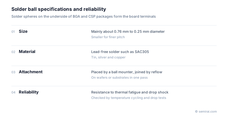
A solder ball is a small sphere of solder attached in a grid to the underside of a ball grid array (BGA) or chip-scale package (CSP). The balls are the package's external terminals: when the board is reflowed they melt and join the package pads to the board pads. Typical diameters run from about 0.76 mm on 1.27 mm pitch down to about 0.25 mm on 0.4 mm pitch.
Also called: BGA ball, solder sphere
Diagram
Ball mounting
Attaching balls to a package is called ball mounting or ball attach. Flux is printed or pin-transferred onto the substrate pads, and a ball mounter places a ball on every pad at once, either by picking them up with a vacuum head or by sweeping them into a stencil with holes. The parts then pass through a reflow oven, where the balls melt and wet the pads. After cleaning, inspection checks for missing balls, diameter and coplanarity, meaning that all ball tips lie in one plane so every joint touches the board.
Wafer-level CSPs receive their balls on the wafer before dicing. Much smaller balls, below about 100 µm, are also used to form bumps for flip-chip connections.
Materials
Since lead was restricted, most balls are tin-silver-copper alloys, of which SAC305 (3% silver, 0.5% copper) is the most common. Low-silver alloys and alloys with small additions are used to improve drop resistance or lower cost. Ball quality depends on sphericity, diameter accuracy to within a few micrometres and low surface oxidation. Copper-core balls, a copper sphere coated with solder, keep a fixed gap between package and board after reflow and are used where stand-off height or current capacity matters.
Reliability
Packages and boards expand at different rates, so every temperature change strains the joints, and repeated cycling grows fatigue cracks. Joint life is evaluated by temperature cycling tests, and handheld products also undergo drop tests because impact can crack the brittle intermetallic layer at the pad. Large packages are often reinforced with underfill resin. Because the joints are hidden under the package, voids and opens are inspected by X-ray. The term solder ball also describes a defect: small stray spheres of solder scattered on a board during reflow.
Japanese companies involved
- Senju Metal Industry makes solder balls, including copper-core balls, along with solder pastes and fluxes.
- Nippon Micrometal makes bonding wire and fine micro balls used for package terminals and bumps.
- Senju Metal Industry · Solder, flux and solder balls
- Nippon Micrometal · Bonding wire and micro balls
FAQ
What is the difference between a solder ball and a bump?
Solder balls are package terminals, about 0.2 to 0.8 mm across, that connect a package to the circuit board. Bumps are much smaller, from tens of micrometres up to about 100 µm, formed on a chip's pads to connect the chip to the package substrate; they may be solder, copper pillars or gold.
Why do solder ball joints fail?
Mostly through thermal fatigue: the package and board expand by different amounts with each temperature swing, and cracks grow through the solder over many cycles. Mechanical shock from drops and board bending can also break joints, usually at the intermetallic layer.
Related pages
Sources
Last updated: November 13, 2026