SEMI E90 (Substrate Tracking)
SEMI E90 is the SEMI standard that defines how production equipment tracks where each individual wafer is and what processing it has received, and reports this to the factory host computer. It is also known as the substrate tracking standard and is one of the GEM300 standards for 300 mm fab automation.
Also called: E90, substrate tracking, wafer tracking
Diagram
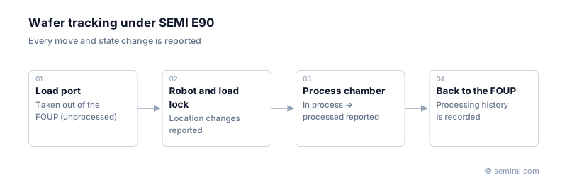
What is tracked
A single tool contains many places a wafer can be: load ports, transfer robots, load locks and several process chambers. SEMI E90 defines these locations and the wafer's processing state, such as not yet processed, in process, processed, or aborted because of an error.
Each time a wafer moves or its state changes, the tool reports it to the host in a standard format.
The standard also lets the host ask the tool at any time where each wafer is, which is useful when operators need to intervene in a running job.
Why wafer-level tracking helps
With per-wafer tracking, the record shows which wafer went through which chamber. When a defect is found later, the responsible tool or chamber is easier to identify, which is the basis of traceability.
If a tool stops partway through a job, the record also shows which wafers are processed and which are not, so recovery can be done correctly. SEMI E90 is used together with SEMI E87, which manages carriers as a whole.
Japanese companies involved
- Japanese equipment makers such as Tokyo Electron implement GEM300 standards, including substrate tracking, in their 300 mm process tools.
- Tokyo Electron (TEL) · Coat/develop, etch and deposition equipment
FAQ
How does SEMI E90 differ from SEMI E87?
SEMI E87 works at the carrier level, verifying a FOUP's ID and the arrangement of wafers inside it. SEMI E90 works at the wafer level, tracking each wafer after it leaves the carrier: where it is inside the tool and what processing it has received. The two are used together.
Why does wafer-level tracking matter?
In a tool with several chambers, wafers from the same lot can be processed in different chambers. If only some wafers turn out defective, chamber-by-chamber records let engineers find the cause quickly and hold back only the affected wafers instead of the whole lot.
Related pages
Sources
Fab infrastructure and equipment parts terms
Last updated: November 1, 2026