Step Coverage
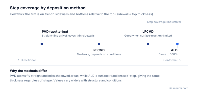
Step coverage is a measure of how evenly a deposited film covers the topography on a wafer. It compares the film thickness on the sidewalls and bottom of a trench or hole with the thickness on the top surface; a film with the same thickness everywhere is called conformal and has close to 100% step coverage.
Also called: conformality, conformal coverage
Diagram
Why deposition methods differ
Physical vapour deposition (PVD) such as sputtering sends atoms in mostly straight lines. The top surface receives the most, while sidewalls and bottoms, partly shadowed, receive less, so step coverage is poor. Chemical vapour deposition (CVD) relies on gas-phase transport and surface reactions, so it coats sidewalls better; low-pressure CVD in the surface-reaction-limited regime is generally better than plasma CVD.
Atomic layer deposition (ALD) is the most conformal. Each precursor pulse saturates the whole surface before the reaction stops, so the film grows by the same amount at the top and the bottom of very deep features.
What poor step coverage causes
If the film is thin on sidewalls or at the bottom, a barrier layer may not stop copper diffusion, an insulator may break down at low voltage, and a conductor may open. If more material builds up at the opening than inside, the opening closes first and leaves a void or a seam in the middle of the feature, which can trap chemicals or raise resistance.
As aspect ratios grow in 3D NAND, DRAM capacitors and gate-all-around transistors, step coverage has become one of the main criteria for choosing a deposition method, often more important than deposition rate.
FAQ
How is step coverage measured?
A cross-section of a test structure is imaged with a scanning or transmission electron microscope, and the sidewall and bottom thicknesses are divided by the top thickness, expressed as a percentage. Bottom coverage is especially important for high-aspect-ratio holes.
Can PVD step coverage be improved?
Yes, to a degree. Long-throw sputtering increases the target-to-wafer distance, and ionised PVD ionises sputtered atoms and draws them vertically into features with a wafer bias. Re-sputtering the bottom film onto the sidewalls also helps. These methods still fall short of ALD for very deep structures.
Comparisons
Related pages
Sources
Last updated: November 1, 2026