CVD (Chemical Vapour Deposition)
CVD (chemical vapour deposition) is a family of thin-film deposition methods in which precursor gases are fed into a chamber and made to react with heat, plasma or light, leaving a solid film on the wafer surface. It is used for insulating, semiconducting and metal films and is one of the core front-end processes.
Also called: chemical vapor deposition, PECVD, LPCVD, APCVD, HDPCVD
Diagram
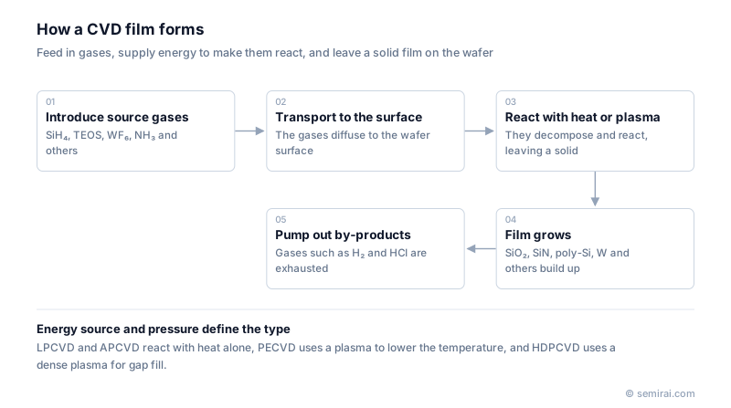
How CVD works
Precursor gases such as silane (SiH₄), TEOS (tetraethoxysilane), tungsten hexafluoride (WF₆) or ammonia flow over the wafer. They diffuse to the surface, decompose or react there, and the solid product stays behind as a film. Gaseous by-products such as hydrogen or hydrogen chloride are pumped away.
Because the film grows by a surface reaction rather than by atoms flying in straight lines, CVD reaches the sidewalls and bottoms of trenches far better than physical vapour deposition (PVD) such as sputtering.
Main types of CVD
The variants differ in pressure and energy source. Atmospheric-pressure CVD (APCVD) is the simplest but generates more particles and now has limited use. Low-pressure CVD (LPCVD) runs at reduced pressure, typically tens of pascals, and gives uniform, high-quality films, often in batch furnaces. Plasma-enhanced CVD (PECVD) uses a plasma to drive the reaction at roughly 200-400°C, so it can be used after metal interconnects are in place. High-density-plasma CVD (HDPCVD) deposits and sputters at the same time to fill narrow gaps.
Typical films include polysilicon for gates and resistors, TEOS-based silicon dioxide for interlayer dielectrics, silicon nitride for spacers and etch stops, and tungsten for filling contacts. Atomic layer deposition (ALD) is a cyclic, self-limiting form of CVD used where films must be only a few nanometres thick and perfectly conformal.
Japanese companies involved
- Tokyo Electron makes single-wafer and batch deposition systems, including CVD and ALD tools used in logic and memory fabs.
- Kokusai Electric specialises in batch vertical furnaces for LPCVD, oxidation and ALD, which process many wafers in one run.
- Tokyo Electron (TEL) · Coat/develop, etch and deposition equipment
- Kokusai Electric · Batch deposition, diffusion and ALD equipment
- ULVAC · Vacuum deposition (sputtering) equipment and vacuum pumps
FAQ
What is the difference between CVD and PVD?
CVD forms the film through a chemical reaction of gases at the surface, so it can coat steep steps and deep holes. PVD knocks or evaporates atoms from a solid source and lets them fly to the wafer, which gives purer metal films but poorer coverage inside narrow features.
Why is PECVD used late in the process?
Once aluminium or copper interconnects and low-k dielectrics are on the wafer, temperatures much above 400°C would damage them. A plasma supplies the energy that heat would otherwise provide, so PECVD can deposit oxide and nitride films at temperatures the interconnects tolerate.
Is ALD a type of CVD?
Yes. ALD uses the same kind of precursor chemistry, but the two reactants are pulsed separately with purges in between, so each cycle adds at most one atomic layer. It trades deposition speed for precise thickness control.
Comparisons
Related pages
- PECVD (Plasma-Enhanced Chemical Vapour Deposition)
- Deposition
- Step Coverage
- Rate-Limiting Step
- Precursor
- ALD (Atomic Layer Deposition)
- Low-k Dielectric
- Plasma (Semiconductor Processing)
- CVD equipment
- Kokusai Electric QUIXACE®
- Kokusai Electric QUIXACE®-II
- Kokusai Electric QUIXACE ULTIMATE®
- Tokyo Electron (TEL) Episode™ 1
Sources
Last updated: November 13, 2026