Interlayer Dielectric (ILD)
An interlayer dielectric (ILD) is the insulating film that separates the metal wiring layers of a chip from each other and fills the spaces between wires in the same layer. It prevents short circuits while keeping the parasitic capacitance between wires small, so it strongly affects signal delay and power in the back end of line (BEOL).
Also called: ILD, inter-metal dielectric, IMD
Diagram
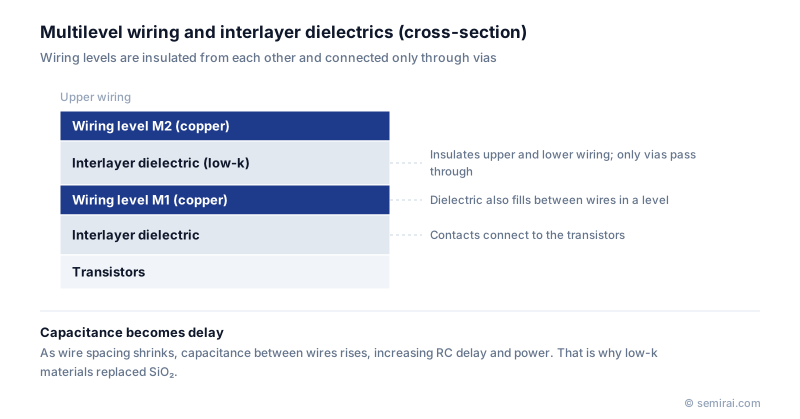
From silicon dioxide to low-k
Early chips used silicon dioxide deposited from TEOS (tetraethoxysilane). To reduce RC delay as wires moved closer together, the industry switched to fluorine-doped oxide (FSG), then to carbon-doped SiOC low-k films, and then to porous low-k films that contain nanometre-scale voids. ILD films are deposited by CVD, mainly plasma-enhanced CVD, or by spin-on coating.
The dielectric below the first metal layer, which surrounds the contacts to the transistors, is called the pre-metal dielectric (PMD) and has different requirements, such as gap fill between gates and resistance to contamination.
What an ILD has to do
Besides low permittivity, an ILD must fill the gaps between wires without voids, withstand chemical mechanical polishing (CMP), resist damage during etching and ashing, and work with the barrier layers that keep copper from diffusing into it. It also has to survive the thermal and mechanical stress of packaging.
These requirements pull against each other. Lowering the permittivity usually makes the film more porous and softer, which reduces its mechanical strength and makes integration harder. Each wiring level therefore uses the dielectric that best balances capacitance and robustness for that level: the tight-pitch lower layers get the lowest k, while thick upper layers often use sturdier oxide.
Japanese companies involved
- Tokyo Electron makes deposition and coating equipment used for interconnect dielectrics, along with the etch tools that pattern them.
- Tokyo Electron (TEL) · Coat/develop, etch and deposition equipment
FAQ
How many ILD layers does a chip have?
One per wiring level plus the pre-metal dielectric. An advanced logic chip can have more than ten metal layers, each separated by its own dielectric, with vias passing through to connect neighbouring levels.
What are etch stop and cap layers in the ILD?
Thin films of silicon nitride or silicon carbonitride are placed between dielectric layers. They stop the via or trench etch at the right depth and cap the copper lines to block diffusion and electromigration. Because they have higher k, they are kept as thin as possible.
What is an air gap?
An air gap is a deliberate void between wires where the dielectric is removed or never deposited. Air has a permittivity close to 1, so capacitance drops sharply, but the structure is weaker and harder to manufacture, so it is used only in selected layers.
Related pages
Sources
Last updated: November 1, 2026