Wire Bonding
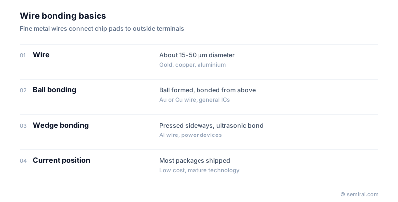
Wire bonding is the back-end process that connects the pads of a semiconductor chip to the leads of a lead frame or the pads of a package substrate with fine metal wires. Wires for typical ICs are about 15-50 µm in diameter. In use since the 1960s, it still connects the majority of packages shipped today.
Also called: ball bonding, wedge bonding, wire bonder
Diagram
Ball bonding and wedge bonding
In ball bonding, the wire passes through a ceramic tool called a capillary. An electric spark melts the wire tip into a small ball, which the capillary presses onto the chip pad with heat, force and ultrasonic energy (the first bond). The capillary then moves to the lead while paying out wire in a controlled loop and presses the wire flat to form the second, or stitch, bond before breaking it off. A modern bonder repeats this in a fraction of a second per wire.
Wedge bonding forms no ball. A wedge-shaped tool presses the wire onto the pad and bonds it ultrasonically, at room temperature. It is mainly used with aluminium wire and, in heavy-wire form, for power semiconductors. Gold was long the standard wire for ball bonding, but copper, palladium-coated copper and silver alloy wires have largely replaced it to reduce cost.
Quality and limits
Bond quality is checked with wire pull tests, which measure the force needed to break the wire, and ball shear tests, which push the ball sideways off the pad. Loop shape matters too: a loop that is too low can touch the die edge, and a long loop can be pushed by flowing mold compound into a neighbouring wire.
Wires are longer than flip-chip bumps, so they add inductance, and pads can only be placed around the die edge. That makes wire bonding a poor fit for very high pin count, high-speed logic. It remains the main method for memory die stacks, sensors, power devices, automotive ICs and most cost-sensitive chips.
Japanese companies involved
- Shinkawa (Yamaha Robotics) and Kaijo make wire bonders.
- Tanaka Precious Metals and Nippon Micrometal make bonding wire in gold, copper and other materials.
- Shinkawa (Yamaha Robotics) · Wire bonders and die bonders
- Kaijo · Wire bonders and ultrasonic cleaning systems
- Tanaka Precious Metals · Bonding wire and precious metal sputtering targets
- Nippon Micrometal · Bonding wire and micro balls
FAQ
What is the difference between wire bonding and flip chip?
In wire bonding the die faces up and its edge pads are connected with fine wires. In flip chip the die is turned face down and joined directly to the substrate through bumps across its surface. Flip chip gives shorter connections and more terminals; wire bonding is cheaper and more flexible.
Why did copper wire replace gold?
Mainly cost: gold prices rose sharply, while copper is far cheaper and conducts better. Copper is harder and oxidises, so it needed bonding in inert gas, adjusted processes and often a palladium coating before it became reliable in high volume.
Comparisons
Related pages
Sources
Last updated: November 13, 2026