QFN (Quad Flat No-lead) Package
A QFN (quad flat no-lead) package is a lead-frame-based package with no leads sticking out of its sides. Instead, flat terminal pads exposed around the edge of its underside are soldered directly to the circuit board, making the package smaller, thinner and lower in parasitic inductance than leaded packages.
Also called: quad flat no-lead, DFN, MLF
Diagram
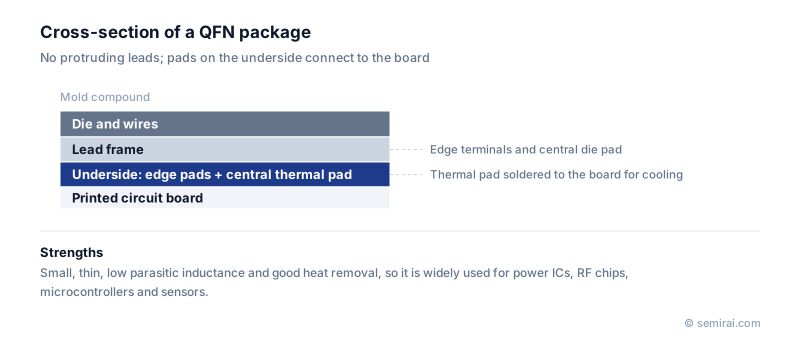
Structure and the exposed pad
Most QFNs have a large exposed die pad in the centre of the underside. The die sits on this pad inside the package, and the pad is soldered to a copper area on the board, usually connected to ground with thermal vias. This gives a short, low-resistance path for heat, so a QFN can dissipate much more power than its size suggests.
Small size, good thermal performance and low inductance make QFNs popular for power management ICs, RF chips, microcontrollers and sensors. The dual-row version is called DFN. Wettable-flank QFNs have plated side notches so that solder fillets can be checked by camera, which automotive customers often require.
How QFNs are made
Most QFNs are produced as molded array packages (MAP). Many dies are attached to a lead-frame strip and connected by wire bonding or, in some cases, flip chip. The whole strip is then encapsulated in one molding step, and a saw or punch separates it into individual packages. This makes QFNs cheap to produce in very high volume.
Quality depends on solder wetting of the exposed terminals, adhesion between mold compound and lead frame, and voids in the solder under the thermal pad, which reduce heat transfer. Because the joints are small and partly hidden, board assembly needs careful stencil design.
Japanese companies involved
- Japanese companies such as Mitsui High-tec and Shinko Electric Industries make lead frames used in QFN and other lead-frame packages.
- Mitsui High-tec · Lead frames
- Shinko Electric Industries · FC-BGA package substrates and lead frames
FAQ
What is the difference between QFN and QFP?
A QFP has gull-wing leads extending from its four sides, which are easy to inspect but take more area. A QFN has its terminals underneath, so it is smaller and has better electrical and thermal performance, but its joints are harder to inspect and rework.
Why must the QFN thermal pad be soldered?
The thermal pad is the main path for heat from the die to the board, and often also the ground connection. If it is not soldered, or contains large voids, the chip can overheat and behave unreliably.
Related pages
Sources
Last updated: November 2, 2026