Lead Frame
A lead frame is the thin, patterned metal sheet that forms the skeleton of conventional packages such as QFP, QFN and SOP. It holds the die on a central pad and provides the leads that are wire-bonded to the chip and later soldered to the printed circuit board.
Also called: leadframe
Diagram
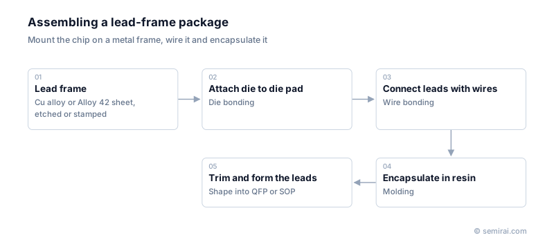
Structure and materials
The die is attached to the die pad, sometimes called the island, at the centre. Around it, inner leads fan inwards towards the die and are connected to the chip's pads by wire bonding. The outer leads, or the exposed pads of a no-lead package, become the external terminals. In QFN packages the die pad is exposed on the underside and also serves as a heat path.
Most lead frames are copper alloy, chosen for its electrical and thermal conductivity. Alloy 42, an iron-nickel alloy whose thermal expansion is close to silicon, is used where matching expansion matters more. The pattern is formed by stamping with precision dies, which is economical for high volumes, or by chemical etching, which allows finer features and quick design changes. Selected areas are plated with silver, or the whole frame with nickel-palladium-gold, so that wires bond well and solder wets the leads.
From strip to package
Lead frames are supplied as strips containing many package sites. Dies are attached and wire-bonded on the strip, the strip is molded, and the packages are then separated. For leaded packages the leads are trimmed and bent to shape; for QFN-type molded array packages the strip is sawn into individual units.
Current development focuses on thinner material, finer lead pitch, plating that resists delamination from mold compound, and frames for power devices that carry high current and heat.
Japanese companies involved
- Mitsui High-tec makes stamped lead frames using its precision tooling, and Shinko Electric Industries also supplies lead frames alongside its package substrates.
- Shinko Electric Industries · FC-BGA package substrates and lead frames
- Mitsui High-tec · Lead frames
FAQ
Are lead frames still used now that BGAs exist?
Yes. Lead-frame packages are cheap, robust and well understood, so they are still used in very large numbers for microcontrollers, analogue and power chips, sensors and automotive devices. BGAs are used where many terminals are needed.
Why are lead frames plated?
Bare copper oxidises, which makes wire bonding and soldering unreliable. Plating with silver at the bonding areas, or with nickel-palladium-gold over the whole frame, gives surfaces that bond and solder well and can improve adhesion to mold compound.
Related pages
Sources
Last updated: November 2, 2026