Gallium Arsenide (GaAs)
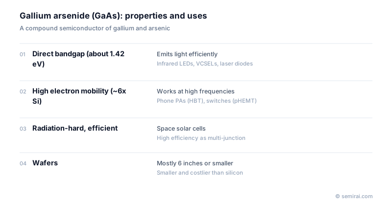
Gallium arsenide (GaAs) is a III-V compound semiconductor made of gallium and arsenic. It has a direct bandgap of about 1.42 eV at room temperature and an electron mobility of about 8,500 cm²/V·s, roughly six times that of silicon. These two properties make it useful both for high-frequency transistors and for devices that emit light.
Also called: GaAs
Diagram
High-frequency and optical uses
In RF electronics, GaAs HBTs (heterojunction bipolar transistors) are widely used as the transmit power amplifiers in mobile phones, and GaAs pHEMTs (pseudomorphic high-electron-mobility transistors) serve as switches and low-noise amplifiers. GaAs and AlGaAs have almost the same lattice constant, so high-quality heterojunctions are easy to make, which is what gives HEMTs and HBTs their performance.
Because the bandgap is direct, GaAs emits light efficiently. It is used for infrared LEDs, laser diodes such as those once used in CD and DVD drives, and VCSELs for face recognition and short-reach data links. GaAs is also the core of multi-junction solar cells for satellites, which combine high efficiency with good radiation tolerance.
Weaknesses and manufacturing
GaAs single crystals are grown by the liquid-encapsulated Czochralski (LEC) or vertical gradient freeze (VGF) method, and wafers are mostly 150 mm (6 inches) or smaller. The material is more brittle than silicon, and its thermal conductivity is only about a third of silicon's, which limits power density. It also lacks a good native oxide, so MOSFETs are impractical; transistors are built as MESFETs with Schottky gates, or as HEMTs and HBTs.
Device layers are grown by MOCVD or MBE epitaxy. Because the material contains arsenic, grinding debris, wastewater and process exhaust must be handled and treated carefully.
Japanese companies involved
- Sumitomo Electric Industries makes GaAs substrates.
- Sumitomo Electric Industries (compound semiconductors) · SiC epitaxial wafers and GaAs and InP substrates
- Murata Manufacturing · Capacitors, RF modules, SAW/BAW filters and MEMS sensors
FAQ
Why are GaAs amplifiers used in phones rather than silicon ones?
At the frequencies and output powers of mobile transmitters, GaAs HBTs deliver higher efficiency and linearity than silicon. The semi-insulating GaAs substrate also reduces losses. Silicon and SOI handle many receive, switch and control functions, so phone front ends combine both.
What is the difference between GaAs and GaN?
GaAs has a bandgap of about 1.42 eV and suits moderate-power RF and infrared light emitters. GaN, at about 3.4 eV, withstands much higher voltages and power, so it is used in base-station amplifiers, power transistors and blue LEDs. The two often coexist in the same radio system.
Related pages
- Compound Semiconductor
- High Electron Mobility Transistor (HEMT)
- Heterojunction
- Arsenic (As)
- Indium Phosphide (InP)
- Gallium Nitride (GaN)
- Substrate
- Lattice Constant
- Compound semiconductor wafers
- Compound semiconductor equipment
- RF semiconductor (GaN/GaAs) equipment
- Sumitomo Electric Industries (compound semiconductors) GaN substrates
- Canon ANELVA EC7400
- Canon ANELVA EC8100
- HORIBA PLATO-MicroScan
Sources
Last updated: November 13, 2026