Copper (Cu)
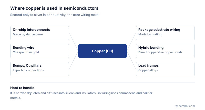
Copper is the metal with atomic number 29 and symbol Cu. It conducts electricity better than any metal except silver, with a resistivity of about 1.7 µΩ·cm at room temperature. In semiconductors it carries current almost everywhere: in on-chip interconnects, bonding wires and bumps, package substrates, and direct chip-to-chip bonds.
Also called: Cu
Diagram
From aluminium to copper interconnects
Chips used aluminium wiring until copper interconnects entered production in the late 1990s, following IBM's announcement in 1997. Copper has lower resistance than aluminium (about 2.7 µΩ·cm) and much better resistance to electromigration, the movement of metal atoms driven by current. Both reduce wiring delay and improve reliability.
Copper is hard to etch with plasma, and it diffuses into silicon and insulators, where it degrades transistors. The damascene process solved both problems. Trenches and vias are first etched into the dielectric, then lined with a barrier metal and a copper seed layer, filled with copper by electroplating and polished flat by CMP. To keep copper away from transistor fabrication, fabs separate copper-handling tools and wafer carriers.
Copper outside the chip and its limits
In packaging, copper bonding wire has largely replaced gold for cost reasons, copper pillars connect flip chips, and package substrates and printed circuit boards use plated copper and copper foil. In advanced packaging, hybrid bonding joins copper pads on two chips directly, without solder. Lead frames are also made of copper alloys.
Copper has limits at the finest dimensions. When lines are only a few tens of nanometres wide or less, electron scattering at grain boundaries and surfaces raises resistivity, and the barrier takes up a large share of the line. Ruthenium and molybdenum are being studied for the narrowest levels.
Japanese companies involved
- JX Advanced Metals makes high-purity copper sputtering targets used to deposit the copper seed layers of interconnects.
- JX Advanced Metals · Sputtering targets and high-purity metals
FAQ
Why is copper treated as a contaminant in fabs?
Copper diffuses very quickly through silicon, and even trace amounts increase leakage and shorten carrier lifetime. Besides wrapping copper wiring in barrier metal, fabs keep copper processes separate from front-end transistor steps, with dedicated tools, carriers and handling rules.
What is the difference between single and dual damascene?
In single damascene, vias and trenches are formed and filled with copper in separate steps. In dual damascene, both are etched first and then filled and polished together, which saves steps and removes an interface. Dual damascene is standard for most copper levels.
Related pages
- Copper Interconnect (Damascene Process)
- Barrier Metal (Diffusion Barrier)
- Hybrid Bonding
- Metal Contamination
- Tungsten (W)
- Plating Additives
- Sputtering Target
- Sputtering targets
- JX Advanced Metals Cu and Ta sputtering targets for semiconductors
- Tanaka Precious Metals Precious metal sputtering targets (melting method)
- Tosoh Metal targets (Mo, Cu, Ti and others)
Sources
Last updated: November 12, 2026