Annealed Wafer
An annealed wafer is a polished silicon wafer that has been heat-treated at around 1,200 °C in hydrogen or argon to remove crystal-originated particles (COPs) near the surface. The result is a defect-free surface layer one to several micrometres deep, achieved at lower cost than growing an epitaxial layer.
Also called: hydrogen-annealed wafer, argon-annealed wafer
Diagram
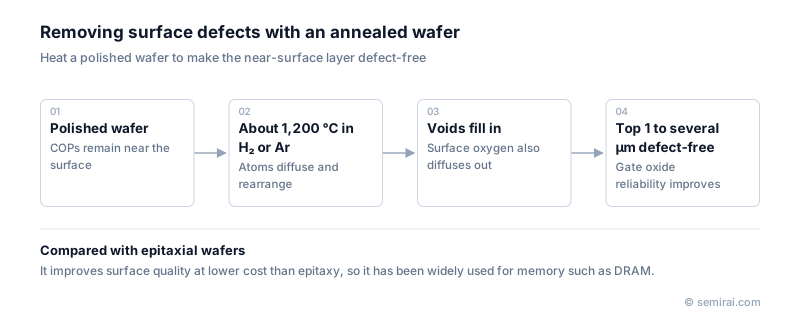
How annealing removes COPs
COPs are tiny octahedral voids formed as vacancies cluster during crystal growth. At high temperature, the thin oxide lining the voids near the surface dissolves, and silicon atoms diffuse and rearrange to fill them. The native oxide on the surface is also removed, and the surface becomes smooth at atomic scale.
Hydrogen and argon behave differently. Hydrogen is strongly reducing and gives a cleaner, smoother surface, but it is flammable, so furnaces need extra safety measures. Argon is inert and easier to handle and helps oxygen diffuse out of the surface to form a denuded zone, but it smooths the surface less than hydrogen.
Where annealed wafers fit
Annealed wafers sit between polished and epitaxial wafers. Polished wafers may contain COPs at the surface; epitaxial wafers have a fully grown single-crystal layer but cost more. By removing COPs while avoiding epitaxy, annealed wafers improve gate oxide integrity (GOI) at a moderate cost, which suited memory such as DRAM.
Since wafer makers learned to grow nearly defect-free crystals by controlling the ratio of pull rate to temperature gradient (V/G), wafers with few COPs can be supplied directly, and annealed wafers are less unique than before. They keep one structural advantage: the surface is defect-free while the bulk can still hold precipitates for gettering.
Japanese companies involved
- SUMCO and Shin-Etsu Chemical include annealed wafers in their silicon wafer product lines alongside polished and epitaxial wafers.
- Kokusai Electric makes vertical batch furnaces of the type used for high-temperature heat treatment of wafers.
- SUMCO · Silicon wafers
- Shin-Etsu Chemical · Silicon wafers, photoresists and photomask blanks
- Kokusai Electric · Batch deposition, diffusion and ALD equipment
FAQ
When is an epitaxial wafer chosen instead?
When the surface layer must be as perfect as possible, or when the doping of the surface layer has to be set independently of the substrate, as in many logic and power devices. If removing COPs is enough and cost is tight, an annealed wafer may be chosen.
Why does the anneal need such a high temperature?
Silicon atoms must diffuse fast enough to fill the voids, and the oxide lining the voids must dissolve. Both happen at a useful rate only well above 1,100 °C, which is why annealing is done at around 1,200 °C.
Comparisons
Related pages
Sources
Last updated: November 13, 2026