Epitaxial Wafer (Epi Wafer)
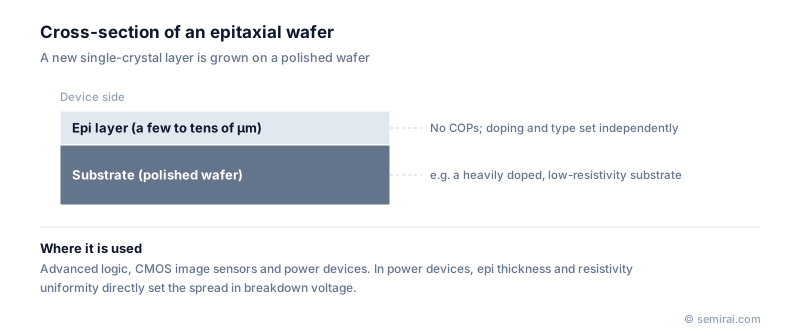
An epitaxial wafer is a polished silicon wafer on which a single-crystal silicon layer, from a few micrometres to several tens of micrometres thick, has been grown from the gas phase. Because the substrate and the grown layer can be doped independently, one wafer can combine a surface that is electrically ideal with a substrate chosen for strength and gettering.
Also called: epi wafer, epitaxial silicon wafer
Diagram
Why chipmakers choose epi wafers
There are three main reasons. First, crystal quality at the surface: the epitaxial layer covers crystal-originated particles (COPs) in the substrate, which improves gate oxide integrity (GOI). Second, freedom in the doping profile: a lightly doped p- layer grown on a heavily doped p+ substrate gives good resistance to latch-up without hurting transistor characteristics. Third, the grown layer contains almost no oxygen, unlike Czochralski (CZ) crystal.
In power devices the epitaxial layer matters even more. The blocking voltage of vertical power MOSFETs and IGBTs is set by the thickness and doping of the drift layer, so the uniformity of epi thickness and resistivity translates directly into device-to-device variation. In silicon carbide (SiC), converting basal plane dislocations from the substrate into less harmful threading edge dislocations during epitaxy is a key to reliability.
How the layer is grown
Silicon epitaxy is normally done one wafer at a time in a single-wafer reactor. The wafer is heated to roughly 1,000-1,150 °C in hydrogen, and a silicon source gas such as trichlorosilane (SiHCl₃) is supplied, so that silicon deposits as a single crystal continuing the substrate's orientation. Dopant gas flows at the same time to set the resistivity. A hydrogen bake before growth removes the native oxide and is essential for a clean starting surface.
The drawbacks are cost and defects. Single-wafer growth takes time, so an epi wafer costs noticeably more than a polished wafer. Contamination or particles on the starting surface can nucleate stacking faults and epi spikes, defects specific to epitaxy.
Japanese companies involved
- Shin-Etsu Chemical and SUMCO make polished and epitaxial silicon wafers for logic, image sensors and power devices.
- NuFlare Technology makes epitaxial growth reactors.
- NuFlare Technology · Electron-beam mask writers, mask inspection and epitaxial reactors
- Shin-Etsu Chemical · Silicon wafers, photoresists and photomask blanks
- SUMCO · Silicon wafers
FAQ
Which chips are usually made on epitaxial wafers?
Advanced logic, CMOS image sensors and power semiconductors are typical users. Many mainstream memory and logic products use polished or annealed wafers instead, because the epitaxial step adds cost that only pays off when the surface quality or doping profile is needed.
What is a p/p+ epitaxial wafer?
It is a lightly doped p-type epitaxial layer on a heavily doped p-type substrate. The low-resistance substrate collects stray current and helps suppress latch-up in CMOS circuits, while transistors are built in the lightly doped layer above it.
What is an epi spike?
It is a small, abnormal local growth that sticks up from the epitaxial surface, usually starting from a particle or contamination on the substrate. Along with stacking faults, it is one of the defects that epi wafer makers inspect for.
Comparisons
Related pages
- Epitaxy (Epitaxial Growth)
- Annealed Wafer
- Silicon Wafer Manufacturing
- SiC Wafer (Silicon Carbide Substrate)
- Gettering
- Power Semiconductor
- Dislocation
- Substrate
- Compound semiconductor substrate equipment (SiC/GaN)
- Daiichi Kiden Solution Growth System
- Fujikoshi Machinery LSL-19A
- Hamai Industries HS1200
- Okamoto Machine Tool Works OGM390NC2HX
Sources
Last updated: November 13, 2026