Interstitial Oxygen (Oi)
Interstitial oxygen (Oi) is oxygen dissolved between lattice sites in silicon grown by the Czochralski method. It comes from the quartz crucible dissolving into the melt, typically at about 10-18 ppma (roughly 5×10¹⁷ to 9×10¹⁷ atoms/cm³). Float zone silicon, grown without a crucible, contains almost none.
Also called: Oi, oxygen concentration in silicon
Diagram
Why oxygen helps
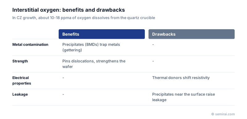
During heat treatment, oxygen precipitates inside the wafer as bulk micro-defects (BMDs). These trap iron, copper and other metals away from the device layer, which is called intrinsic gettering. Dissolved oxygen also pins dislocations, which makes the wafer stronger and less prone to slip in high-temperature steps.
Why oxygen can hurt
Heat treatment around 450 °C can turn oxygen clusters into thermal donors, which add electrons and shift the resistivity away from the target. Precipitates close to the surface can cause junction leakage. Wafers are therefore often treated so that oxygen diffuses out of the top layer, leaving a precipitate-free denuded zone over a bulk that still contains BMDs.
The right concentration depends on the device. Logic and memory wafers aim for a balance between gettering and strength. Power devices and radiation detectors, which need long minority carrier lifetime, often use float zone wafers with almost no oxygen.
How it is controlled and measured
Oxygen content is set during crystal growth through crucible rotation, crystal rotation, furnace pressure and argon flow. Magnetic CZ (MCZ), which applies a magnetic field to suppress melt convection, reduces oxygen pick-up and makes its distribution more uniform. Oi is normally measured by Fourier-transform infrared spectroscopy (FT-IR), which detects the absorption of the Si-O-Si bond.
Japanese companies involved
- Shin-Etsu Chemical and SUMCO set the oxygen concentration of their CZ wafers to customer specifications, balancing gettering, strength and electrical stability.
- Shin-Etsu Quartz Products makes high-purity quartz glass, the material of the crucibles that are the source of the oxygen.
- Shin-Etsu Quartz Products · High-purity quartz glass parts and crucibles
- Shin-Etsu Chemical · Silicon wafers, photoresists and photomask blanks
- SUMCO · Silicon wafers
FAQ
Why are ppma figures sometimes inconsistent between sources?
Converting the FT-IR absorption into a concentration uses a calibration factor, and different standards (older ASTM, newer ASTM, JEIDA) use different factors. Values should always be compared using the same standard.
What is a denuded zone?
It is a layer near the wafer surface where oxygen has diffused out during heat treatment, so no precipitates form. It keeps the transistor region clean while the bulk below still holds precipitates for gettering.
Related pages
Sources
Last updated: November 13, 2026