Silicon Wafer Manufacturing
Silicon wafer manufacturing is the sequence that turns high-purity polysilicon into mirror-polished single-crystal wafers ready for device fabrication. It covers crystal growth, shaping, slicing, lapping or grinding, etching, polishing, cleaning and inspection, and it is carried out by specialist wafer makers before chip fabs start their front-end process.
Also called: wafer production, wafer process, wafer making
Diagram
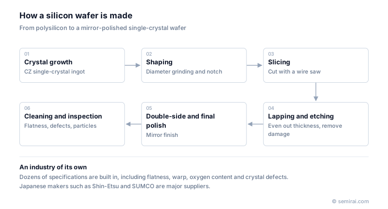
The main steps
First a single-crystal ingot is grown, usually by the Czochralski method from a melt in a quartz crucible, or by the float zone method when low oxygen and high resistivity are needed. The ingot is ground to an exact diameter, a notch or flat is cut to mark the crystal orientation, and a wire saw slices it into thin wafers.
As-sliced wafers have saw marks, a damaged surface layer and thickness variation. Lapping or double-side grinding sets the thickness and flatness, chemical etching removes the damaged layer, and double-side polishing followed by final polishing produces a mirror surface. The edge is also shaped and polished to reduce chipping and particles. After final cleaning, every wafer is inspected, laser-marked with an ID and packed in shipping boxes (FOSBs).
Why the specifications matter
A wafer is controlled by dozens of parameters. Flatness affects the focus margin in lithography, nanotopography affects CMP uniformity, bow and warp affect handling and chucking, interstitial oxygen sets gettering ability and strength, and crystal defects such as COPs affect gate oxide integrity.
Different products follow from the same base process: polished wafers, epitaxial wafers with a grown single-crystal layer, annealed wafers with a defect-free surface, SOI wafers with a buried insulator, and reclaimed test wafers. SiC, GaN and sapphire substrates are produced in separate lines.
Japanese companies involved
- Shin-Etsu Chemical (through Shin-Etsu Handotai) and SUMCO are two of the main silicon wafer manufacturers, producing polished, epitaxial, annealed and SOI wafers.
- Japanese equipment makers supply many of the tools in this chain, for example wire saws from Komatsu NTC and Takatori, and lapping and polishing machines from SpeedFam and Hamai Industries.
- Komatsu NTC · Wire saws for slicing silicon and SiC ingots
- Takatori · Wire saws, dicing-related equipment and bonding/debonding systems
- SpeedFam · Wafer polishing and lapping equipment
- Hamai Industries · Lapping and polishing machines for wafers
- Shin-Etsu Chemical · Silicon wafers, photoresists and photomask blanks
- SUMCO · Silicon wafers
FAQ
How is a wafer maker different from a foundry?
A wafer maker produces blank wafers with no circuits; it is a materials supplier. A foundry buys those wafers and builds circuits on them through repeated lithography, deposition and etching. They sit at different layers of the supply chain.
Why does a blank wafer need so many specifications?
Each property shows up later as a process window or yield problem. A wafer that is slightly too uneven may defocus in lithography, one with the wrong oxygen level may warp or getter poorly, and one with surface defects may give weak gate oxides.
Related pages
- Silicon Ingot
- Czochralski Process (CZ Method)
- Wire Saw
- Lapping
- Wafer Flatness (TTV / SFQR / GBIR)
- Epitaxial Wafer (Epi Wafer)
- Silicon Wafer
- Final Polishing
- Crystal growth furnaces
- Wafer polishing and edge grinding equipment
- Komatsu NTC GCG300
- SpeedFam FAM59SPAW / FAM50SPAW
- SpeedFam UH-I-8100 / UH-I-8800
- SpeedFam WIFG-300
Sources
Last updated: November 13, 2026