Gettering
Gettering is the set of techniques that draw metal impurities such as iron, copper and nickel away from the near-surface region where transistors are built, and trap them at sites where they cause no harm. It is a basic part of wafer and process design, because metals cause junction leakage and short carrier lifetime.
Also called: intrinsic gettering, extrinsic gettering, IG, EG
Diagram
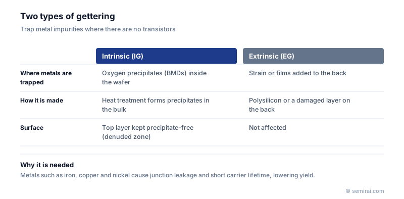
Intrinsic and extrinsic gettering
Intrinsic gettering (IG) uses the oxygen already present in CZ silicon. A sequence of heat treatments makes the oxygen precipitate inside the wafer as bulk micro-defects (BMDs). Their strained surroundings act as sinks where metal atoms collect.
Extrinsic gettering (EG) adds trapping sites from outside, usually on the back of the wafer. Examples are mechanical damage, a polysilicon film, or heavy phosphorus diffusion. The metals diffuse to the backside during high-temperature steps and stay there.
Keeping the surface clean
Gettering only helps if the precipitates are kept away from the active layer. A high-temperature step drives oxygen out of the top few micrometres so that no precipitates form there, leaving a denuded zone above a precipitate-rich bulk. Designing the oxygen content and the thermal history so that both layers form is a joint task for wafer suppliers and chipmakers.
Thinned wafers bring a new problem: grinding the back removes much of the bulk where BMDs sit. One answer is to leave a controlled strained layer on the ground surface that still traps metals while keeping the wafer strong.
Japanese companies involved
- Shin-Etsu Chemical and SUMCO design the oxygen content and heat treatment of their CZ wafers so that the wafers provide intrinsic gettering in customers' processes.
- DISCO offers grinding wheels that leave a gettering layer on the back of thinned wafers, so that the wafer keeps a trap for metals after most of the bulk has been removed.
- DISCO · Dicing, grinding and polishing equipment
- Shin-Etsu Chemical · Silicon wafers, photoresists and photomask blanks
- SUMCO · Silicon wafers
FAQ
Why are metal impurities so harmful?
Metals such as iron, copper and nickel form deep energy levels in the silicon band gap. These act as recombination and generation centres, which raise junction leakage and shorten minority carrier lifetime. Very small concentrations are enough to cause yield loss.
Where do the metals come from?
From equipment parts, chemicals, handling and some process steps such as ion implantation or metal deposition. Fabs work hard to prevent contamination, but gettering provides a safety margin for what still reaches the wafer.
Comparisons
Related pages
Sources
Last updated: November 2, 2026