Gate Oxide (Gate Dielectric)
Gate oxide is the thin insulating film between the gate electrode and the semiconductor channel of a MOSFET. It lets the gate voltage control the channel through an electric field while blocking current between gate and channel. For decades it was thermally grown silicon dioxide (SiO₂); advanced transistors now use hafnium-based high-k dielectrics.
Also called: gate dielectric, gate insulator
Diagram
What the gate oxide does
The gate, oxide and channel form a capacitor. A voltage on the gate induces charge in the channel and switches the transistor on. The thinner the dielectric, the larger this capacitance and the stronger the gate's control over the channel, which raises drive current and helps suppress short-channel effects. Scaling the gate oxide has therefore gone hand in hand with shrinking the transistor.
The film must also have very few defects, a clean interface with the channel and high resistance to breakdown, because it is stressed by a strong electric field throughout the chip's life. Breakdown and threshold voltage drift caused by charge trapping in the dielectric are key reliability tests.
From thick SiO₂ to the tunnelling limit
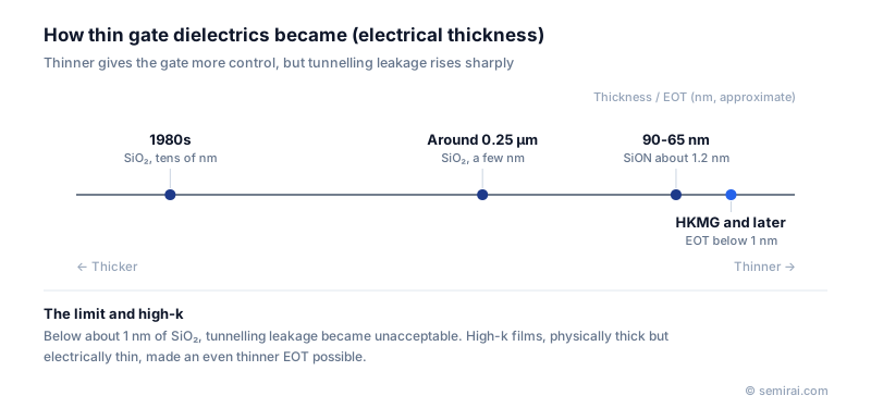
Thermal oxidation of silicon produces SiO₂ with an exceptionally good interface, which is one of the main reasons silicon became the dominant semiconductor. Gate oxides went from tens of nanometres in early MOS chips to a few nanometres around the 0.25 µm generation. Nitrogen was then added to form silicon oxynitride (SiON), which blocks boron diffusion from the gate and raises permittivity slightly.
At the 90 nm and 65 nm nodes the oxynitride was only about 1.2 nm thick, a handful of atomic layers. At that thickness electrons tunnel directly through the film, and gate leakage current increases exponentially as the film is thinned further, so SiO₂ could not be scaled any more.
High-k dielectrics and EOT
The solution was to replace SiO₂ with a material of higher permittivity, mainly hafnium oxide (HfO₂). A high-k film can be physically thicker, which cuts tunnelling, while giving the capacitance of a much thinner SiO₂ layer. This electrical thickness is expressed as equivalent oxide thickness (EOT). Intel introduced high-k metal gate (HKMG) at 45 nm in 2007, and foundries adopted it at around 28 nm. A thin SiO₂-based interfacial layer is still kept under the high-k film, because HfO₂ directly on silicon gives a poor interface.
Japanese companies involved
- Tokyo Electron and Kokusai Electric make batch furnaces and ALD equipment used for gate oxidation and for depositing high-k dielectrics.
- Tokyo Electron (TEL) · Coat/develop, etch and deposition equipment
- Kokusai Electric · Batch deposition, diffusion and ALD equipment
FAQ
Why is it still called gate oxide when high-k materials are used?
The name dates from the era of SiO₂ and stuck. Engineers often say gate dielectric or gate insulator instead, and HfO₂ is in fact an oxide too, so the old name is still accurate in a literal sense.
Do all transistors on a chip use the same gate oxide thickness?
No. Chips usually have thin-oxide core transistors for logic and thicker-oxide transistors for input/output circuits and analogue blocks that run at higher voltages. Power devices and many mature-node chips still use thermally grown SiO₂ tens of nanometres thick.
What is time-dependent dielectric breakdown (TDDB)?
TDDB is the gradual creation of defects in a dielectric under constant voltage until a conductive path forms and the film breaks down. It is tested at elevated voltage and temperature and extrapolated to operating conditions to confirm the gate dielectric will last the product's lifetime.
Related pages
Sources
Last updated: November 2, 2026