Bulk Silicon
In semiconductors, 'bulk' means the interior of a material as opposed to its surface, interfaces or thin films. Bulk silicon in particular is an ordinary wafer made entirely of single-crystal silicon, with transistors built directly in its surface, as distinct from silicon-on-insulator (SOI), which has a buried insulating layer.
Also called: bulk substrate, bulk wafer, bulk CMOS
Diagram
Bulk as the interior of a material
Engineers speak of bulk properties to mean the properties of the material itself, away from the influence of the surface. Bulk mobility is the carrier mobility deep inside the crystal, and bulk recombination is recombination of carriers inside the material rather than at the surface. Outside physics the word also means goods in large quantities, but in semiconductor writing it almost always means the interior.
In MEMS, bulk micromachining means etching deep into the silicon substrate itself to form structures, while surface micromachining shapes thin films deposited on top.
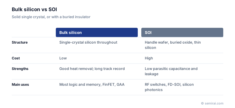
Bulk silicon vs SOI
Bulk wafers are cheaper than SOI and have a long manufacturing track record, so most logic and memory is made in bulk CMOS. Most leading-edge FinFET and gate-all-around (GAA) transistors are also built on bulk substrates.
The key difference is whether the transistor is connected to the substrate underneath. In bulk silicon, a p-n junction forms between each device and the substrate. That brings junction capacitance and leakage, parasitic coupling between neighbouring devices that can lead to latch-up, and greater sensitivity to radiation-induced soft errors. SOI isolates the device layer with a buried oxide and suppresses these effects, but the wafer costs more.
Japanese companies involved
- Shin-Etsu Chemical and SUMCO supply bulk silicon wafers, both polished and epitaxial, as well as SOI wafers.
- Shin-Etsu Chemical · Silicon wafers, photoresists and photomask blanks
- SUMCO · Silicon wafers
FAQ
If SOI has fewer parasitic effects, why is most logic made on bulk silicon?
Cost and ecosystem. Bulk wafers are cheaper, design kits and process know-how are mature, and FinFET and GAA structures already give strong gate control on bulk. SOI is used where its advantages are decisive, such as RF switches, FD-SOI for low-power chips and silicon photonics.
Does bulk silicon handle heat better than SOI?
Yes. The buried oxide in SOI conducts heat poorly, so heat generated in the thin device layer escapes less easily. In bulk silicon the heat flows straight into the thick crystal underneath.
Comparisons
Related pages
Sources
Last updated: November 2, 2026