Crystal Structure
Crystal structure is the regular, repeating three-dimensional arrangement of atoms in a solid. It is described by a small repeating unit, the unit cell, whose edge lengths are the lattice constants. In semiconductors the crystal structure shapes the band structure and carrier mobility, how wafers cleave and etch, and which materials can be grown on top of each other.
Also called: crystal lattice, unit cell
Diagram
Lattices, unit cells and Miller indices
A crystal can be described as a lattice, a grid of identical points repeating in space, with the same group of atoms (the basis) placed at every point. Stacking the unit cell in three directions rebuilds the whole crystal. There are 14 possible lattice types, grouped into seven crystal systems such as cubic and hexagonal.
Planes and directions in a crystal are named with Miller indices. In a cubic crystal, (100) is a cube face, (110) cuts diagonally through two faces and (111) cuts across three corners; braces such as {111} denote the whole family of equivalent planes. These labels appear on every wafer specification.
The structures that matter in semiconductors
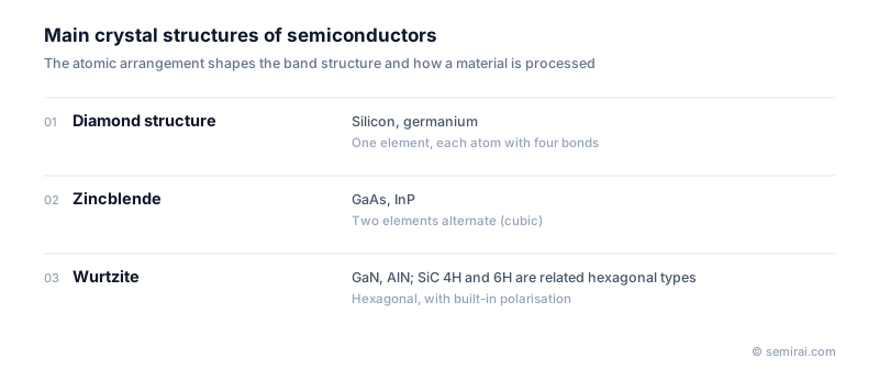
Silicon and germanium have the diamond structure: each atom forms four covalent bonds to neighbours at the corners of a tetrahedron. It can be pictured as two face-centred cubic lattices offset by a quarter of the cube diagonal. Silicon's cubic cell, 0.543 nm on a side, holds eight atoms, giving about 5×10²² atoms per cm³.
The zincblende structure has the same geometry with two elements alternating, as in GaAs and InP. The wurtzite structure stacks the same tetrahedra in a hexagonal sequence; GaN, AlN and ZnO take this form, and its built-in polarisation creates the electron gas used in GaN HEMTs. SiC exists in many polytypes that differ only in stacking order, such as cubic 3C and hexagonal 4H and 6H; 4H-SiC is used for power devices.
Why orientation matters in manufacturing
Wafers are sliced from single crystals grown mostly by the Czochralski method and cut to a specified orientation. CMOS wafers are almost always (100), because the silicon-oxide interface on that plane has the fewest electrical defects; (111) silicon is used as a substrate for GaN-on-Si growth. Orientation also controls processing: alkaline etchants such as KOH etch {111} planes far more slowly than others, which MEMS makers use to form V-grooves with 54.7° sidewalls. When one crystal is grown on another, a mismatch in lattice constants introduces strain and, beyond a critical thickness, dislocations.
Japanese companies involved
- Shin-Etsu Chemical and SUMCO grow single-crystal silicon ingots and slice them into wafers of specified orientation.
- Sumitomo Electric supplies zincblende GaAs and InP substrates, and Rigaku makes X-ray diffraction systems used to check crystal orientation and quality.
- Shin-Etsu Chemical · Silicon wafers, photoresists and photomask blanks
- SUMCO · Silicon wafers
- Sumitomo Electric Industries (compound semiconductors) · SiC epitaxial wafers and GaAs and InP substrates
- Rigaku · X-ray metrology and thermal analysis
FAQ
Why does silicon take the diamond structure?
Silicon has four valence electrons and forms four equivalent covalent bonds pointing to the corners of a tetrahedron. Repeating that tetrahedral bonding in three dimensions produces the diamond structure, the same arrangement carbon adopts in diamond.
What is a polytype?
A polytype is one of several crystal structures of the same compound that differ only in how identical atomic layers are stacked. SiC has more than 200 known polytypes; 4H-SiC is preferred for power devices because it combines a wide band gap with higher and less direction-dependent electron mobility than 6H-SiC.
Do polycrystalline and amorphous silicon have a crystal structure?
Polycrystalline silicon consists of many small crystals (grains), each with the diamond structure but oriented differently, separated by grain boundaries. Amorphous silicon has no long-range order. Both are used in thin films, such as gate electrodes and display transistors, but transistors in ICs are built in single-crystal silicon.
Related pages
Sources
Last updated: November 2, 2026