Crystal Plane Orientation
Crystal plane orientation tells which crystal plane a silicon wafer's surface is cut along, expressed in Miller indices such as (100), (110) or (111). It is a basic wafer specification because surface atom density, oxidation and etch rates, carrier mobility and the quality of the silicon/oxide interface all change with orientation.
Also called: surface orientation, wafer orientation
Diagram
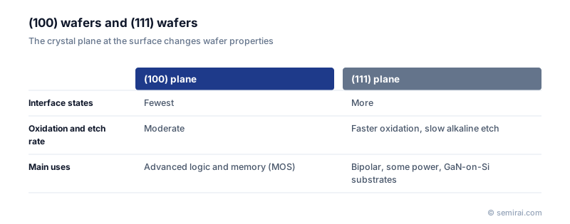
Why most chips use (100) wafers
MOS transistors depend on a clean interface between silicon and the gate insulator. On the (100) plane, the density of interface states between silicon and silicon dioxide is the lowest of the common orientations, which gives stable threshold voltages and good electron mobility. For this reason almost all CMOS logic and memory is built on (100) wafers.
(111) wafers oxidise faster and have more interface states, but they were historically used for bipolar transistors and are still used for some power devices. Silicon (111) is also the usual substrate for GaN-on-silicon epitaxy, because its surface has the threefold symmetry that matches the hexagonal GaN crystal.
Marking and using the orientation
The orientation of the surface is only half the story; tools also need to know the in-plane crystal directions. Smaller wafers carry an orientation flat, a straight cut on the edge whose position and the presence of a secondary flat once also indicated the conductivity type. Wafers of 200 mm and 300 mm have a small notch instead. Equipment uses the flat or notch to align the wafer so that patterns line up with crystal directions.
Orientation matters directly in processing. Alkaline wet etching of silicon stops on {111} planes, so the angle of etched walls in MEMS depends on the wafer's surface plane and the alignment of the mask to the notch. Wafers are sometimes cut a few degrees off the exact plane (off-cut) to control epitaxial growth.
Japanese companies involved
- Shin-Etsu Chemical's wafer business and SUMCO supply silicon wafers in the orientations, notch positions and off-cut angles that chipmakers specify.
- Shin-Etsu Chemical · Silicon wafers, photoresists and photomask blanks
- SUMCO · Silicon wafers
FAQ
Can transistors be made faster by changing orientation?
Yes, for holes. Hole mobility is higher on (110) surfaces and along certain directions, so some designs rotate the channel direction or use hybrid orientations. In FinFETs the side walls of the fins, not the wafer surface, form the channel, so the fin direction sets which plane the current flows on.
How is the orientation of a wafer checked?
It is measured by X-ray diffraction, which detects the angle at which a known set of crystal planes reflects X-rays. The same method is used when the ingot is ground and the notch or flat is cut, so that the marks match the true crystal directions.
Related pages
Sources
Last updated: November 2, 2026