Plastic Deformation
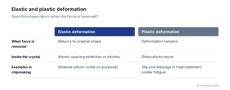
Plastic deformation is a change of shape that remains after the applied force is removed, as opposed to elastic deformation, which disappears when the force is released. It begins when the stress exceeds the yield stress. Pressing clay leaves a dent; a spring springs back. In crystals, plastic deformation happens mainly through the movement of dislocations.
Also called: permanent deformation, yielding
Diagram
How crystals deform plastically
A dislocation is a line defect in the crystal lattice. Under stress it can glide along particular crystal planes, called slip planes. Each time a dislocation passes, one part of the crystal shifts relative to the other by one atomic spacing, and the shift stays after the stress is removed. Plastic deformation is the sum of many such slip events.
Silicon is hard and brittle at room temperature: it cracks before it deforms plastically. Above roughly 600 to 700 °C, however, dislocations can move, and silicon begins to deform plastically under stress.
Slip and warpage in wafer processing
High-temperature steps such as diffusion furnaces, rapid thermal processing and epitaxial growth create two kinds of stress in a wafer: thermal stress from temperature differences across the wafer, and stress from the wafer's own weight at the points where it is supported. If these stresses are too high, dislocations are generated and move, leaving defects known as slip lines and permanent warpage. Slip can cause leakage and makes the wafer harder to pattern flat.
Larger wafers are heavier and develop larger temperature differences, so support designs, edge rings and ramp rates for heating and cooling are tuned to keep stress below the level that causes slip.
Plastic deformation in packaging
In packages, solder joints deform plastically every time the temperature changes, because the chip and the board expand by different amounts. Repeated cycles slowly grow cracks until the joint fails by thermal fatigue. Temperature-cycle testing evaluates this, and the relation between plastic strain and cycles to failure is described by the Coffin-Manson law. Plastic deformation is also used on purpose: in wire bonding, a gold or copper ball is squashed onto the pad to form the bond.
Japanese companies involved
- Shin-Etsu Chemical's wafer business and SUMCO supply epitaxial and annealed silicon wafers, whose high-temperature processing must be controlled to avoid slip.
- SUMCO · Silicon wafers
- Shin-Etsu Chemical · Silicon wafers, photoresists and photomask blanks
FAQ
Is strained silicon a form of plastic deformation?
No. Strained silicon deliberately keeps the silicon channel elastically strained to raise carrier mobility. If the strain were relieved by dislocations, which is plastic relaxation, the benefit would be lost and defects would appear, so the strained layers are kept below their critical thickness.
How are slip lines detected on a wafer?
Slip appears as sets of straight lines along crystal directions, often near the edge or support points. They can be seen with X-ray topography, by optical inspection after a defect-revealing etch, or as small surface steps measured by wafer inspection tools.
Related pages
Sources
Last updated: November 2, 2026