Single Crystal
A single crystal is a solid in which the atoms keep one continuous, regular arrangement throughout the whole piece, with no grain boundaries where the crystal orientation changes. It is also called a monocrystal. Semiconductor devices are, as a rule, built on single-crystal silicon wafers.
Also called: monocrystal, monocrystalline
Diagram
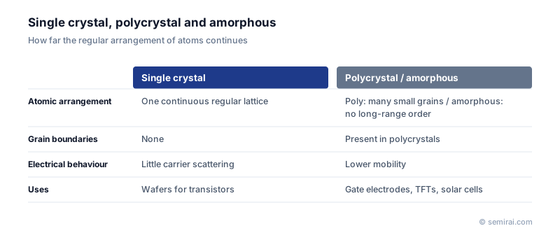
Single crystal, polycrystal and amorphous
A polycrystalline material is made of many small crystals, called grains, each with its own orientation. Where the grains meet there are grain boundaries, regions of disturbed bonding. An amorphous material has no long-range order at all: atoms are bonded to their neighbours but the pattern does not repeat over distance.
Grain boundaries and disorder scatter carriers and act as recombination and trapping sites, which lowers mobility and raises leakage. High-performance transistors therefore need a single-crystal channel. Polycrystalline and amorphous silicon still have important roles where these losses are acceptable, such as gate electrodes, thin-film transistors for displays and some solar cells.
Growing single-crystal silicon
Silicon for wafers is grown mainly by the Czochralski (CZ) method. A small seed crystal is dipped into molten silicon in a quartz crucible and slowly pulled up while rotating, so the melt freezes onto it with the same orientation. Ingots of 300 mm diameter are grown this way and then sliced, ground and polished into wafers.
The float-zone (FZ) method melts a narrow zone of a polysilicon rod with a radio-frequency coil and moves it along the rod. No crucible touches the melt, so FZ silicon contains much less oxygen and is used for some power devices and detectors. CZ silicon is used for most logic and memory because it can be made in large diameters at lower cost, and its oxygen content also helps trap metal impurities.
Japanese companies involved
- Shin-Etsu Chemical's wafer business and SUMCO grow single-crystal silicon ingots and process them into wafers.
- Tokuyama produces the high-purity polycrystalline silicon used as the raw material for crystal growth.
- Shin-Etsu Chemical · Silicon wafers, photoresists and photomask blanks
- SUMCO · Silicon wafers
- Tokuyama · Polysilicon and electronic chemicals
FAQ
Does a single crystal have no defects at all?
No. A single crystal can still contain point defects, dislocations and impurities; it only lacks grain boundaries. Modern silicon wafers are grown free of dislocations, but small voids and oxygen precipitates are controlled by the growth conditions and later heat treatments.
Can layers grown on a wafer also be single crystal?
Yes. In epitaxial growth, a new layer is deposited so that its atoms continue the arrangement of the substrate. The epitaxial layer is a single crystal with the same orientation, which is how device layers of silicon, SiC and GaN are formed.
Related pages
Sources
Last updated: November 2, 2026