EOT (Equivalent Oxide Thickness)
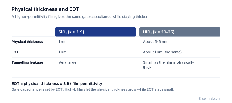
EOT (equivalent oxide thickness) expresses the electrical thickness of a gate dielectric as the thickness of silicon dioxide that would give the same capacitance. It is calculated as EOT = t × (3.9 / k), where t is the physical thickness and k the relative permittivity, so a higher-k film has a smaller EOT.
Also called: equivalent oxide thickness, electrical oxide thickness
Diagram
Why EOT is used
Gate capacitance controls how strongly the gate voltage turns the channel on. With silicon dioxide alone, raising capacitance meant thinning the oxide, but below about 1 nm direct tunnelling leakage becomes unacceptable. EOT lets engineers compare any dielectric on the same scale: what matters electrically is the EOT, while what controls leakage is largely the physical thickness.
For example, 5 nm of HfO₂ with k ≈ 22 has an EOT of about 5 × 3.9 / 22 ≈ 0.9 nm. The film behaves like 0.9 nm of SiO₂ while being more than five times thicker, which suppresses tunnelling by orders of magnitude.
What sets the EOT of a real gate stack
A real stack is not only high-k. A thin interfacial layer of silicon oxide or oxynitride sits between the channel and the HfO₂, and its EOT adds in series. Because this layer has low k, every few tenths of a nanometre of it costs a large share of the total. Thinning it reduces EOT but tends to increase interface trap density and reduce carrier mobility, so it is a careful trade-off.
Advanced logic nodes run with EOTs below 1 nm. Further reduction comes from minimising the interfacial layer, for example by plasma nitridation or scavenging techniques, and from raising the effective k of the high-k layer through doping or crystal phase control, all with atomic-scale ALD control.
FAQ
How is EOT measured?
The standard electrical method is capacitance-voltage (C-V) measurement on a MOS capacitor, from which EOT is extracted after quantum-mechanical corrections. Physical thickness is checked by ellipsometry, X-ray reflectivity (XRR) and cross-sectional transmission electron microscopy (TEM), and composition by X-ray photoelectron spectroscopy (XPS).
Is a smaller EOT always better?
A smaller EOT raises gate capacitance, which improves drive current and gate control of short channels. But pushing it down by thinning the films increases leakage and can degrade mobility and reliability, so each technology node targets an EOT that balances performance, power and lifetime.
What is CET compared with EOT?
Capacitance equivalent thickness (CET) is extracted from the measured capacitance in inversion and therefore also includes the effects of the channel's quantum confinement and any gate depletion. It is slightly larger than EOT, which describes the dielectric alone.
Related pages
Sources
Last updated: November 2, 2026