MOSFET (Metal-Oxide-Semiconductor Field-Effect Transistor)
A MOSFET (metal-oxide-semiconductor field-effect transistor) is a transistor in which the voltage on a gate electrode turns the current between source and drain on and off. It is the basic switching element of modern integrated circuits: CPUs, memories and smartphone SoCs contain billions of them, and discrete power MOSFETs switch large currents in power supplies and motor drives.
Also called: MOS transistor, nMOS, pMOS
Diagram
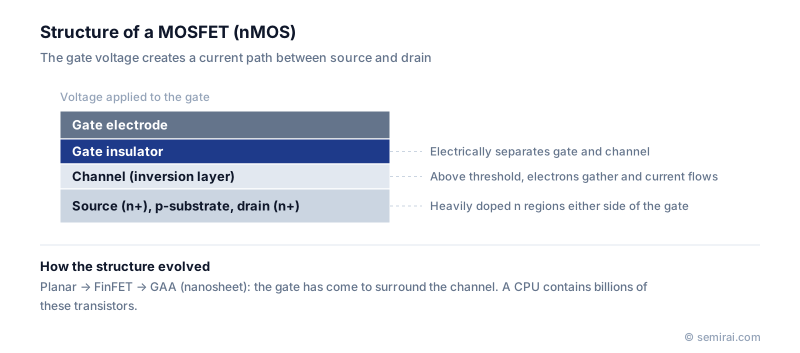
How a MOSFET works
The name describes the stack: a metal (or conductive) gate, a thin insulating oxide, and the semiconductor below. In an n-channel MOSFET (nMOS) on p-type silicon, the source and drain are heavily doped n-type regions on either side of the gate. When the gate voltage exceeds the threshold voltage, it attracts electrons to the surface under the gate, forming an inversion layer that connects source and drain. Remove the voltage and the channel disappears. Because the gate draws almost no current, the MOSFET is a voltage-controlled device.
A p-channel MOSFET (pMOS) works the same way with holes. Combining nMOS and pMOS so that one is off whenever the other is on gives CMOS logic, which draws significant current only while switching. That low power is why CMOS became the standard for digital circuits.
How the MOSFET has changed with scaling
Shrinking the gate made short-channel effects worse, so the structure evolved from planar transistors to FinFETs and then to gate-all-around nanosheets. The gate oxide became so thin, around 1 nm of silicon dioxide, that leakage forced a switch to high-k dielectrics and metal gates. Manufacturing steps such as sidewall spacers, lightly doped drain (LDD) regions and shallow source/drain junctions remain critical to performance and yield.
Japanese companies involved
- Toshiba Electronic Devices & Storage, ROHM and Renesas Electronics make discrete and integrated power MOSFETs for automotive, industrial and consumer equipment.
- Japanese makers are also active in SiC MOSFETs for high-voltage power conversion, including ROHM, Mitsubishi Electric and Fuji Electric.
- Toshiba Electronic Devices & Storage · Power MOSFETs, IGBTs and discrete semiconductors
- ROHM · SiC and silicon power devices, analog ICs
- Renesas Electronics · Microcontrollers, automotive SoCs, analog and power chips
- Mitsubishi Electric (power devices) · IGBT and SiC power modules, RF and optical devices
- Fuji Electric (power semiconductors) · IGBT modules and SiC power devices
FAQ
What is the difference between nMOS and pMOS?
nMOS conducts with electrons and turns on with a positive gate voltage; pMOS conducts with holes and turns on with a negative gate voltage relative to its source. Electrons move faster than holes in silicon, so pMOS devices are often drawn wider to match nMOS drive.
What is the threshold voltage?
It is the gate voltage at which the channel forms and current starts to flow. Designers choose threshold voltages to balance speed against leakage: a lower threshold switches faster but leaks more when the transistor is off.
Is a power MOSFET different from a logic MOSFET?
The principle is the same, but power MOSFETs use vertical or trench structures with thick drift regions so they can block tens to thousands of volts and carry large currents.
Related pages
Sources
Last updated: November 2, 2026