Insulating Film (Dielectric Film)
An insulating film, usually called a dielectric film in English, is a thin layer that does not conduct electricity. In chips it electrically separates wires, transistor electrodes and devices. Common materials are silicon dioxide (SiO₂), silicon nitride (SiN), silicon oxynitride (SiON), high-k materials such as HfO₂ and low-k materials such as SiOC.
Also called: dielectric film, insulator film
Diagram
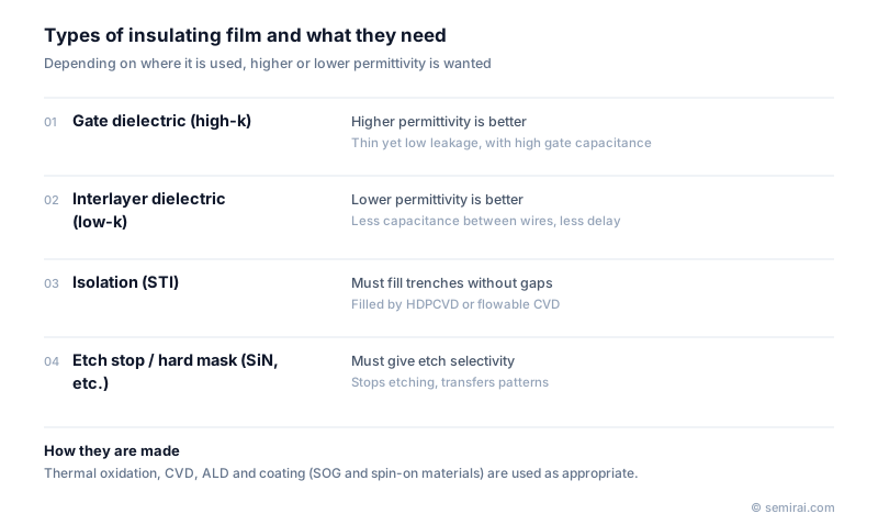
Different jobs, opposite requirements
A gate dielectric must couple the gate's electric field strongly into the channel while staying thin and leak-tight, so a higher permittivity is better and leading-edge transistors use high-k films. An interlayer dielectric between wires should add as little capacitance as possible to reduce RC delay and power, so a lower permittivity is better. SiO₂ has k ≈ 3.9, low-k films reach roughly 2.5-3.0, and air gaps approach 1.
Other dielectric roles include filling isolation trenches (STI), stopping etches, serving as hard masks, blocking moisture and mobile ions as a passivation layer, and forming the capacitor dielectric in DRAM. Each role weights permittivity, gap fill, etch selectivity and density differently.
How dielectric films are made and checked
Dielectric films are formed by thermal oxidation, chemical vapour deposition (plasma-enhanced, low-pressure and high-density-plasma CVD), atomic layer deposition, and coating methods such as spin-on glass and polyimide.
Key properties include breakdown field, which is about 10 MV/cm for good SiO₂, leakage current, permittivity, film stress, and time-dependent dielectric breakdown (TDDB), the lifetime of a film under constant voltage stress. As interconnect dielectrics become thinner and, in the case of low-k, softer, keeping enough mechanical strength for CMP and packaging has become a challenge as well.
Japanese companies involved
- Tokyo Electron makes CVD, ALD and furnace systems used to deposit many of the dielectric films in a chip.
- Tokyo Electron (TEL) · Coat/develop, etch and deposition equipment
FAQ
What is the difference between a gate dielectric and an interlayer dielectric?
Both insulate, but their goals are opposite. The gate dielectric should have high permittivity so that a physically thicker film still gives high capacitance. The interlayer dielectric should have low permittivity so that neighbouring wires couple as little as possible.
Why is silicon nitride used alongside silicon oxide?
Silicon nitride etches very differently from oxide, so it makes a good etch stop and hard mask. It is also denser and blocks moisture, mobile ions and oxygen, which makes it useful for passivation, spacers and as an oxidation mask. Its higher permittivity, about 7, keeps it out of places where capacitance must be low.
Related pages
- Interlayer Dielectric (ILD)
- Low-k Dielectric
- Gate Dielectric Scaling
- Oxide Film (Silicon Dioxide)
- Passivation
- Time-Dependent Dielectric Breakdown (TDDB)
- Air Gap Dielectric
- Spin-On Glass (SOG)
- CVD equipment
- PECVD equipment
- ALD equipment
- Oxide CMP equipment
- Tokyo Electron (TEL) Episode™ 1
- Tokyo Electron (TEL) Episode™ 2 DMR
- Tokyo Electron (TEL) NT333™
- Tokyo Electron (TEL) TELINDY PLUS™ IRad™
Sources
Last updated: November 13, 2026