Gate Dielectric Scaling
Gate dielectric scaling is the effort to make the gate insulator of a MOSFET thinner so that the gate controls the channel more strongly. A thinner insulator improves transistor performance, but below a certain thickness electrons tunnel straight through it and gate leakage rises steeply. The industry resolved this trade-off with the concept of equivalent oxide thickness (EOT) and high-k dielectric materials.
Also called: gate oxide scaling, EOT scaling
Diagram
From silicon dioxide to high-k
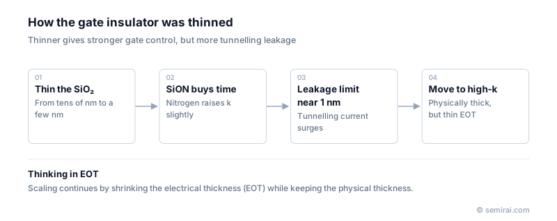
For decades the gate insulator was silicon dioxide (SiO2), thinned from tens of nanometres to a few. Adding nitrogen to form SiON raised the dielectric constant slightly and extended its life. At around 1 nm, only a few atomic layers, tunnelling leakage became unacceptable. In 2007 Intel introduced high-k metal gates (HKMG) at 45nm, replacing SiO2 with a hafnium-based oxide and the polysilicon gate with metal. Hafnium oxide (HfO2) has a dielectric constant of roughly 20-25, against 3.9 for SiO2.
EOT expresses the electrical thickness of any gate insulator as the thickness of SiO2 that would give the same capacitance: EOT = physical thickness × (3.9 / k). A high-k film can therefore be physically several times thicker, which blocks tunnelling, while behaving electrically like a much thinner oxide. A thin SiO2-like interfacial layer usually remains between the silicon and the high-k film, and it sets a floor on how far EOT can fall.
Scaling in GAA transistors
In gate-all-around nanosheets, the high-k film and metal gate must be deposited uniformly on all sides of every sheet, including the narrow gaps between stacked sheets. Only atomic layer deposition (ALD) can coat these spaces conformally with sub-nanometre control. Researchers are also studying adding elements such as lanthanum to hafnium oxide and other higher-k materials to reduce EOT further while keeping leakage and threshold voltage in check.
Japanese companies involved
- Tokyo Electron and Kokusai Electric make ALD and other deposition equipment used to form thin dielectric films.
- ULVAC-PHI makes X-ray photoelectron spectroscopy (XPS) instruments used to analyse the composition of thin gate dielectric films.
- Kokusai Electric · Batch deposition, diffusion and ALD equipment
- ULVAC-PHI · Surface analysis instruments (XPS, TOF-SIMS)
- Tokyo Electron (TEL) · Coat/develop, etch and deposition equipment
FAQ
Why can't the gate oxide simply be made thinner?
Below about 1-2 nm of SiO2, electrons tunnel quantum-mechanically through the insulator, and gate leakage current rises exponentially as thickness falls. That leakage wastes power even when the transistor is idle, so further thinning of SiO2 became impractical.
Do power devices face the same issue?
Their concern is different. SiC MOSFETs use relatively thick gate oxides, and the main challenge is the density of defects at the oxide-SiC interface, which lowers channel mobility and shifts the threshold voltage.
Related pages
Sources
Last updated: November 2, 2026