Gate Stack
A gate stack is the complete set of thin films that forms the gate of a MOSFET. In advanced logic it consists, from the silicon upwards, of an interfacial oxide layer, a hafnium-based high-k dielectric, one or more work-function metal layers and a low-resistance fill metal, each only nanometres thick.
Also called: HKMG gate stack, transistor gate stack
Diagram
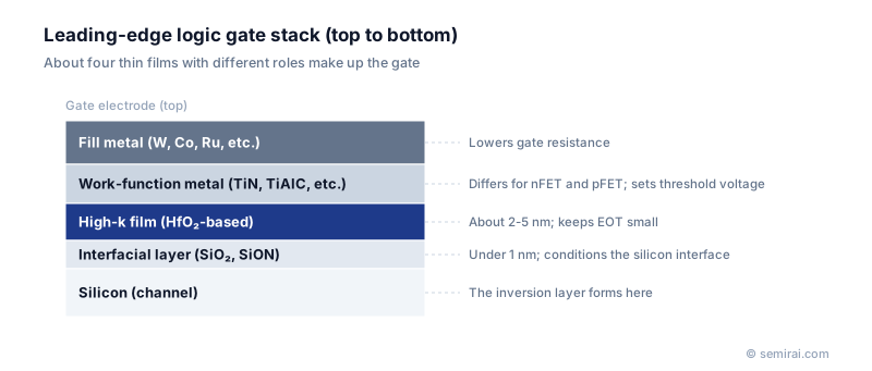
What each layer does
The interfacial layer, usually silicon oxide or oxynitride less than 1 nm thick, gives a clean interface with few traps so that carriers in the channel keep their mobility. The high-k layer, typically 2-5 nm of HfO₂-based material, provides high capacitance with low leakage and keeps the equivalent oxide thickness small.
The work-function metals, for example TiN, TaN or aluminium-containing TiAlC, are chosen differently for n-type and p-type transistors and largely set their threshold voltages. The fill metal, such as tungsten, cobalt or ruthenium, lowers the gate resistance so that the gate can switch quickly. Designing a gate stack means optimising all these layers together, because changes in one shift the behaviour of the others.
How the stack is built
In current logic the stack is formed by the replacement metal gate process. After the dummy polysilicon gate is removed, the interfacial layer is grown by oxidation or plasma treatment, HfO₂ is deposited by atomic layer deposition, work-function metals are added in several ALD steps with patterning to separate n- and p-type regions, and the fill metal is deposited by CVD or ALD. Chemical mechanical polishing then removes the excess.
In gate-all-around nanosheet devices the stack has to wrap each stacked sheet completely, so all layers must coat narrow gaps conformally and the fill must contain no voids. Thickness and composition are monitored with ellipsometry, X-ray reflectivity and TEM analysis.
Japanese companies involved
- Tokyo Electron makes ALD, CVD and etch systems used to build gate stacks in logic fabs.
- Tokyo Electron (TEL) · Coat/develop, etch and deposition equipment
FAQ
Why are there several work-function metal layers?
A single chip needs n-type and p-type transistors and often several threshold-voltage options for each. Different combinations and thicknesses of work-function metals, sometimes with dipole-forming layers near the high-k film, give each device type its own threshold voltage.
What did a gate stack look like before HKMG?
Before 2007 a typical gate stack was simply a thermally grown silicon dioxide or oxynitride layer topped by doped polysilicon, sometimes with a metal silicide on top to lower resistance. The move to high-k and metal gates turned a two-layer structure into a multi-layer one.
Related pages
Sources
Last updated: November 2, 2026