HBM4 (High Bandwidth Memory 4)
HBM4 is the generation of high-bandwidth memory standardised by JEDEC as JESD270-4 in April 2025. It doubles the interface of each DRAM stack from 1,024 to 2,048 bits, giving up to about 2 TB/s per stack at the standard's 8 Gb/s per pin, and is built for the next wave of AI accelerators.
Diagram
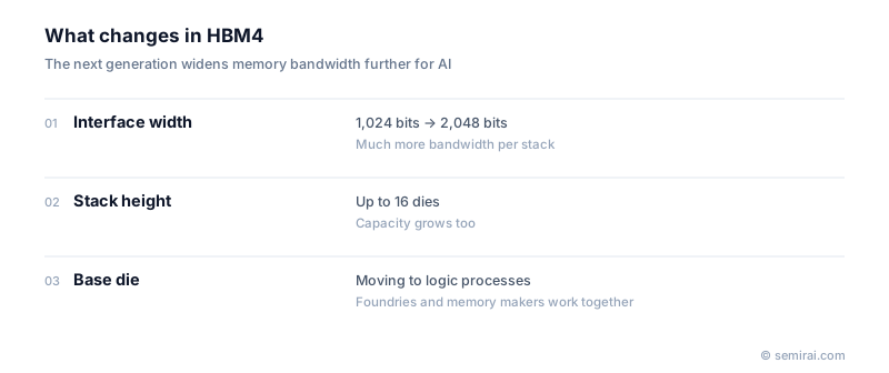
What changes from HBM3E
The wider interface is the headline change, but it is not the only one. The number of independent channels per stack doubles from 16 to 32, each with two pseudo-channels. The standard allows stacks of 4, 8, 12 or 16 DRAM dies with 24 Gb or 32 Gb per die, so a 16-high stack of 32 Gb dies reaches 64 GB.
The base die at the bottom of the stack is changing too. In earlier generations it mainly buffered input and output; for HBM4, memory makers are working with foundries to build base dies on logic processes and add functions that customers ask for.
Manufacturing
Each DRAM die in an HBM stack is thinned to a few tens of micrometres, connected through thousands of through-silicon vias and bonded to the die below. More dies, thinner wafers and denser bumps make wafer thinning, TSV formation, bonding and known-good-die testing the steps that decide yield. SK hynix announced in September 2025 that it had completed HBM4 development and prepared for mass production, and Samsung and Micron are developing their own.
Japanese companies involved
- DISCO's grinders, polishers and dicing saws are used to thin and singulate the DRAM wafers that go into HBM stacks.
- Advantest supplies memory test systems used to test DRAM dies before and after stacking.
FAQ
How fast is HBM4?
The JEDEC standard specifies up to 8 Gb/s per pin over a 2,048-bit interface, about 2 TB/s per stack. Memory makers have announced parts running faster than the standard speed.
Why does AI need HBM?
Large AI models move huge amounts of data between memory and the processor. HBM sits on the same package as the accelerator and offers a far wider interface than ordinary DRAM, so the processor spends less time waiting for data.
What is the base die?
It is the logic die at the bottom of the HBM stack that connects the DRAM dies to the processor. HBM4 base dies are increasingly made on foundry logic processes.
Comparisons
Related pages
Sources
Last updated: November 2, 2026