CoWoS (Chip on Wafer on Substrate)
CoWoS (chip on wafer on substrate) is a 2.5D advanced packaging technology developed and offered by TSMC. Logic dies, such as a GPU, and stacks of high-bandwidth memory (HBM) are mounted side by side on an interposer with very fine wiring, which is then attached to a package substrate, giving short, extremely wide connections between processor and memory.
Also called: chip on wafer on substrate, CoWoS-S, CoWoS-L, CoWoS-R
Diagram
How CoWoS is built
The name describes the order of assembly. First the chips are bonded with micro-bumps onto an interposer while it is still part of a wafer (chip on wafer). The interposer carries several layers of fine wiring and through-silicon vias (TSVs) that pass signals down to its back side. The wafer is then thinned and diced, and each interposer with its dies is mounted onto an organic build-up substrate (on substrate), which connects to the circuit board through solder balls.
Because the interposer wiring is made with wafer-fab tools, its line pitch is far finer than any organic substrate, allowing thousands of connections between the processor and each HBM stack.
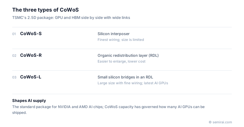
The three CoWoS variants
CoWoS-S uses a full silicon interposer and offers the finest wiring. Its size was originally limited by the reticle, and TSMC has enlarged it by stitching exposures to several times the reticle area. NVIDIA's H100 and AMD's MI300 use CoWoS-S.
CoWoS-R replaces silicon with an organic redistribution layer (RDL) interposer, which is cheaper and easier to make large but has coarser wiring. CoWoS-L embeds small local silicon interconnect bridges in an RDL interposer, giving fine wiring only where dies meet while allowing a very large package. NVIDIA's Blackwell GPUs use CoWoS-L.
Why it matters for AI
Large AI accelerators need several terabytes per second of memory bandwidth, which only HBM placed millimetres from the processor can provide. Since demand for AI hardware surged in 2023, CoWoS capacity has been one of the main constraints on AI GPU supply, and TSMC has expanded its advanced packaging plants in Taiwan accordingly.
Japanese companies involved
- Ajinomoto's ABF film is the insulating material used in the build-up package substrates under CoWoS assemblies, and IBIDEN makes such large FC-BGA substrates.
- DISCO's grinders and dicing saws are used to thin and singulate interposer wafers.
FAQ
What is the difference between CoWoS and InFO?
Both are TSMC packaging families. CoWoS uses an interposer and targets large, high-power HPC and AI chips. InFO (integrated fan-out) builds redistribution wiring directly around the die without an interposer, giving thinner, cheaper packages first used for smartphone processors.
Is CoWoS 2.5D or 3D packaging?
CoWoS is usually called 2.5D because the dies sit side by side on an interposer rather than on top of each other. HBM stacks inside a CoWoS package are themselves 3D stacks of DRAM dies, and TSMC combines CoWoS with its SoIC 3D stacking in some products.
Do other companies offer similar packaging?
Yes. Intel uses EMIB bridges embedded in the substrate for 2.5D connections, Samsung offers I-Cube with silicon interposers, and OSATs such as ASE and Amkor provide interposer and bridge-based packaging. TSMC remains the main supplier for leading AI accelerators.
Comparisons
Related pages
Sources
Last updated: November 2, 2026