HBM (High Bandwidth Memory)
HBM (high bandwidth memory) is a type of DRAM in which several memory dies are stacked vertically and connected with through-silicon vias (TSVs). Each stack talks to the processor over a very wide bus, 1,024 bits in most generations, which gives far higher bandwidth per watt than conventional DDR or GDDR memory.
Also called: high bandwidth memory, stacked DRAM
Diagram
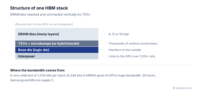
How an HBM stack is built
A stack consists of a base die (also called a logic die) with several thinned DRAM dies above it, typically 8, 12 or 16 high in recent products. Thousands of TSVs run vertically through the DRAM dies and carry data, address and power between layers. The dies are joined with microbumps and a non-conductive film or molded underfill, and hybrid bonding is being developed for taller stacks.
The stack sits next to the processor on a silicon interposer or bridge, as in TSMC's CoWoS. The short, dense wiring of the interposer is what makes a 1,024-bit interface practical; on a normal circuit board so many signals would be impossible to route.
Generations and standards
HBM is standardised by JEDEC. The first generation was adopted in 2013, followed by HBM2, HBM2E, HBM3 and HBM3E, each raising the data rate per pin. HBM4 doubles the interface to 2,048 bits per stack. A processor uses several stacks at once, so total bandwidth reaches several terabytes per second; NVIDIA's H100 SXM, for example, has 80 GB of HBM3 with about 3.35 TB/s.
Making HBM is hard because each extra layer multiplies the risk of a bad die or bond. Wafer thinning, TSV formation, die stacking and inspection all have to work at high yield.
Japanese companies involved
- No Japanese company currently makes HBM, but DISCO's grinders and dicing machines are used to thin and separate the DRAM wafers before stacking, and Japanese materials makers supply films, underfills and mold compounds used in the stack.
- DISCO · Dicing, grinding and polishing equipment
FAQ
Why do AI chips need HBM?
Training and running large AI models moves huge amounts of data between memory and compute units. If memory cannot keep up, the processor sits idle, so bandwidth often limits performance more than raw compute does. HBM gives the highest bandwidth available in a package.
Who makes HBM?
Three DRAM makers produce it: SK hynix, Samsung Electronics and Micron Technology. Securing enough HBM supply has been a key concern for AI accelerator makers.
How is HBM different from GDDR?
GDDR chips sit on the circuit board around a GPU and use narrow, very fast interfaces. HBM sits inside the package on an interposer and uses a very wide, slower-per-pin interface, which gives more bandwidth at lower power but costs more.
Comparisons
Related pages
Sources
Last updated: November 13, 2026