Hexagonal Boron Nitride (hBN)
Hexagonal boron nitride (hBN) is a layered material in which boron and nitrogen atoms alternate in the same hexagonal sheet structure as graphene. It is white and structurally similar to graphene, hence the nickname 'white graphene', but it is an insulator with a bandgap of about 6 eV.
Also called: h-BN, white graphene
Diagram
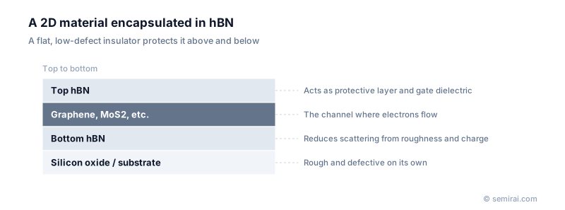
Why hBN matters for 2D materials
In research on two-dimensional materials, hBN has become the standard substrate and insulator. Its sheets are atomically flat, have no dangling bonds on the surface, and contain few charge traps. Silicon dioxide, the usual substrate, has surface roughness and trapped charges that scatter electrons in a channel only a few atoms thick.
Placing graphene or molybdenum disulphide (MoS2) on hBN, or sandwiching it between two hBN flakes, removes much of that scattering and reveals the material's intrinsic performance. The encapsulated sandwich structure is now used very widely in laboratories. High-quality hBN crystals grown at Japan's National Institute for Materials Science (NIMS) have been supplied to research groups around the world for this purpose.
From research to production
For future transistors built from 2D materials, hBN is studied as a gate dielectric and protective layer. The main hurdle is growing uniform, low-defect films over a full wafer; small exfoliated flakes work in the lab but cannot be used in manufacturing. Chemical vapour deposition and other growth methods are being developed to close that gap.
Boron nitride itself is not new to industry. As a powder or ceramic, it has long been used as an electrically insulating material that conducts heat well, in thermal fillers and in parts for high-temperature equipment.
Japanese companies involved
- Japan's National Institute for Materials Science (NIMS) developed high-pressure growth of high-purity hBN crystals, which became a standard material in 2D materials research worldwide.
- Denka makes inorganic fillers, including boron nitride powders, used in thermally conductive insulating materials.
FAQ
How is hBN different from graphene?
Both are stacks of hexagonal sheets. Graphene is pure carbon with essentially no bandgap, so it conducts electricity. In hBN, boron and nitrogen alternate, which opens a large bandgap of about 6 eV and makes it an insulator.
Why is hBN lattice-matched to graphene?
The in-plane lattice constant of hBN differs from graphene's by only about 2%. This close match is why graphene on hBN can form long-period moiré patterns when the layers are slightly twisted, a feature used in physics research.
Related pages
Sources
Last updated: November 12, 2026