Pre-Amorphization Implant (PAI)
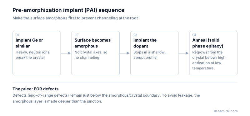
A pre-amorphization implant (PAI) is a pretreatment in which heavy, electrically neutral ions such as germanium or silicon are implanted before the dopant to make the surface layer amorphous on purpose. With no crystal order left, the following dopant implant cannot channel, and the layer regrows during annealing in a way that activates dopants well.
Also called: pre-amorphisation, PAI, Ge PAI
Diagram
What PAI gives
Channeling needs open crystal directions. Once the surface is amorphous, a following boron implant forms a near-Gaussian profile with no deep tail, giving a shallow, abrupt junction. This is more reliable than tilting the wafer and avoids the shadowing that large tilt angles cause in high-aspect-ratio structures.
During annealing the amorphous layer recrystallises by solid phase epitaxy (SPE), growing from the crystal below as a seed at relatively low temperature. Dopant atoms are captured on lattice sites as the interface sweeps through, so high activation is reached at lower temperature, which saves thermal budget.
The price: end-of-range defects
Just beyond the amorphous/crystal boundary the implant leaves an excess of silicon interstitials. After annealing they collect into dislocation loops called end-of-range (EOR) defects. If these defects lie inside the depletion region of the junction, they cause leakage current. The amorphous layer is therefore designed to be deeper than the junction so that the defects sit outside the depletion region.
In advanced logic, PAI, the dopant implant and a spike, flash or laser anneal are tuned together as one recipe.
Japanese companies involved
- Sumitomo Heavy Industries Material Solutions (formerly SMIT) and Nissin Ion Equipment make ion implanters used for both PAI and the dopant implants that follow.
- Nissin Ion Equipment · Ion implanters
- Sumitomo Heavy Industries Material Solutions (formerly SMIT) · Ion implanters
FAQ
Why is germanium used for PAI?
Germanium is in the same group as silicon, so it is electrically neutral and does not act as a dopant. It is also heavy, so a modest dose is enough to amorphise the surface. Silicon itself is sometimes implanted for the same reason.
Does PAI also reduce transient enhanced diffusion?
It can, but it does not remove it. The amorphous layer prevents channeling, yet the interstitials beyond the boundary can still drive boron diffusion during annealing. Carbon co-implantation is often added to capture these interstitials.
How deep is the amorphous layer?
It depends on the ion, energy and dose and is chosen for each process. The rule is that it must reach deeper than the final junction so that the end-of-range defects stay out of the depletion region.
Related pages
Sources
Last updated: November 2, 2026