Ion Channeling
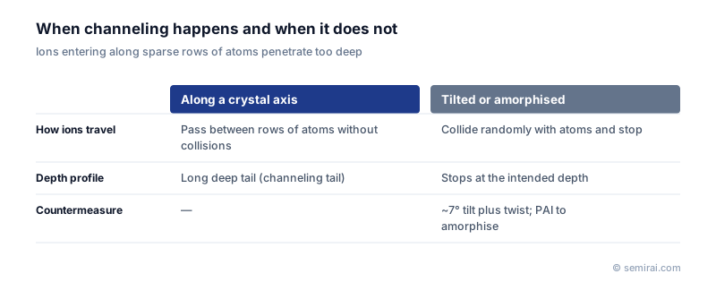
Ion channeling is the effect in which implanted ions enter single-crystal silicon along a crystal axis where the atoms are sparsely arranged and travel much deeper than expected, with few collisions. It appears as a long channeling tail in the depth profile and makes junctions deeper and less predictable than designed.
Also called: channelling, channeling tail
Diagram
Why it happens
Silicon is a crystal, so the density of atoms depends on the direction of view. Looking along major axes such as <100> or <110>, the rows of atoms leave open channels between them. An ion entering such a channel is steered by gentle electrostatic deflections from the rows of atoms and loses energy slowly, so it can reach several times the depth of an ion that enters in a random direction.
Channeling weakens as the dose rises, because the implant itself damages the crystal and gradually makes it amorphous. The early and late parts of the same implant therefore see different crystal conditions, which makes the tail hard to control.
How it is suppressed
The usual method is to tilt the wafer, often by about 7 degrees, and also rotate it in plane (the twist angle, often around 22 degrees) so that the beam avoids all major crystal directions. Tilting has a cost: tall features cast shadows, and dopants do not reach areas behind them. In dense, high-aspect-ratio structures the tilt therefore cannot be large.
The other method is a pre-amorphization implant (PAI). Heavy ions such as germanium destroy the crystal order in the surface layer before the dopant implant. With no crystal axes left, channeling cannot occur, which is why PAI is standard for shallow junctions at advanced nodes.
Japanese companies involved
- Nissin Ion Equipment and Sumitomo Heavy Industries Material Solutions (formerly SMIT) make ion implanters whose end stations control wafer tilt and twist angles to manage channeling.
- Sumitomo Heavy Industries Material Solutions (formerly SMIT) · Ion implanters
- Nissin Ion Equipment · Ion implanters
FAQ
Why is the tilt angle often about 7 degrees?
It is large enough to take the beam well away from the main crystal axis of a (100) wafer, yet small enough to limit shadowing by features on the surface. The twist angle is chosen together with it so that the beam also misses other low-index planes.
Is channeling ever useful?
Yes, outside device manufacturing. In Rutherford backscattering analysis, comparing aligned and random spectra shows how much of a crystal has been damaged or where impurity atoms sit in the lattice.
Does channeling matter for heavy ions?
Less. Heavy ions such as arsenic quickly damage and amorphise the crystal near the surface, which closes the channels. Light ions such as boron cause little damage and channel strongly.
Related pages
Sources
Ion implantation and thermal processing terms
Last updated: November 2, 2026