Spike Anneal
A spike anneal is a rapid thermal processing (RTP) heat treatment that ramps a wafer up very quickly, passes through the peak temperature with essentially no hold time and immediately cools it. By keeping the time near peak temperature to about a second, it supplies the heat needed to activate implanted dopants while minimising their diffusion, and it became the standard post-implant activation anneal.
Also called: spike RTA, spike rapid thermal anneal
Diagram
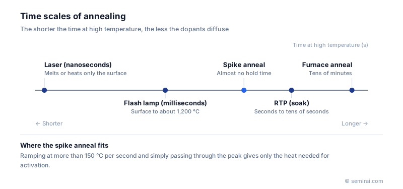
Why the profile is a spike
Activating dopants needs temperatures of roughly 1,000 °C or more, but every second at that temperature lets them diffuse and deepen the junction. Conventional rapid thermal anneals hold the peak for several seconds or more, a 'soak'. A spike anneal instead ramps up at roughly 150-250 °C per second, turns around at the peak and cools straight away, so the temperature-time curve looks like a spike. Its effective duration is commonly described as the time spent within about 50 °C of the peak, typically one to two seconds.
Cooling relies largely on the wafer radiating heat and is usually slower than heating, so tool design focuses on getting heat out as well as in.
What the equipment needs
Spike anneals run in single-wafer RTP chambers heated by banks of tungsten-halogen lamps. The wafer rests on a low-thermal-mass support so it can cool quickly, and multi-zone lamp control with pyrometers measuring wafer temperature keeps the whole wafer within a few degrees. Fast ramps create temperature differences that can cause slip, crystal planes sliding under stress, and patterned wafers absorb and emit heat unevenly, so temperature control and uniformity are the central engineering problems.
Limits and successors
The spike's time scale is its limit. As gate lengths fell below a few tens of nanometres, even one second of diffusion became too much for the shallowest junctions. Flash lamp anneals, which heat only the surface for milliseconds, and laser anneals, from millisecond scanning to nanosecond pulses, took over the most demanding steps. In practice spike and millisecond anneals are often combined: a lower-temperature spike repairs damage and a millisecond flash pushes activation higher.
RTP chambers serve other steps too, such as silicide formation, rapid thermal oxidation and post-deposition film anneals, all following the same idea of giving only the heat that is needed.
Japanese companies involved
- Ushio makes lamps used as heat sources in thermal processing, and has developed flash lamp technology for millisecond annealing.
- Ushio · Light sources and exposure systems for packaging
FAQ
What problem does a spike anneal solve?
It reconciles two conflicting needs: high temperature for dopant activation and minimal time at that temperature to avoid diffusion. Removing the hold at peak cuts the thermal budget sharply compared with soak anneals or furnaces, while still reaching the temperature at which dopants move onto lattice sites.
How is wafer temperature measured during a spike?
Contact sensors are too slow, so RTP tools use pyrometers that read the infrared radiation from the wafer backside. The reading depends on the wafer's emissivity, which varies with films and doping, so tools correct for emissivity and are calibrated with thermocouple wafers and test implants.
Related pages
- Dopant Activation
- Thermal Budget
- Pre-Amorphization Implant (PAI)
- Ramp Rate
- Transient Enhanced Diffusion (TED)
- Boron (B)
- Fick's Laws of Diffusion
- Sheet Resistance (Rs)
- Rapid thermal processing (RTP) equipment
- Kokusai Electric MARORA®
- Kokusai Electric TANDUO
- Koyo Thermo Systems (JTEKT Thermo Systems) RLA-1200
- Koyo Thermo Systems (JTEKT Thermo Systems) RLA-3100
Sources
Last updated: November 13, 2026