Implant Dose
Implant dose is the total number of ions implanted per unit area of the wafer in ion implantation, expressed in atoms/cm². While the acceleration energy sets how deep the ions go, the dose sets how many go in. Being able to set the two independently is the main reason ion implantation replaced thermal diffusion for doping.
Also called: dose, ion dose, implantation dose
Diagram
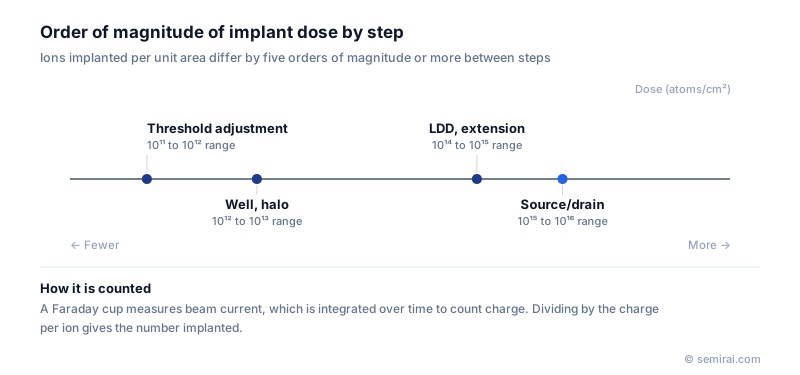
How dose is controlled
An implanter measures dose by counting charge. Faraday cups collect the ion beam beside or behind the wafer and measure its current; integrating the current over time gives the total charge, and dividing by the charge of each ion gives the number of ions. The beam is stopped when the target dose is reached, so the implanter is in effect a precise charge counter.
Several effects can spoil the count. Secondary electrons knocked out of the cup must be suppressed, and ions that pick up an electron from residual gas become neutral and are no longer counted, which implanters correct for using the beamline pressure. Positive charge also builds up on insulating films on the wafer. It can damage thin gate oxides, so implanters neutralise the wafer with an electron flood or plasma flood during implantation.
Typical doses by step
Doses differ by orders of magnitude between steps. Threshold-voltage adjustment uses about 10¹¹ to 10¹² atoms/cm², wells and halo implants about 10¹² to 10¹³, lightly doped drain extensions about 10¹⁴ to 10¹⁵, and source/drain and contact regions 10¹⁵ to 10¹⁶. These ranges explain why fabs use medium-current implanters for low and medium doses and high-current implanters for the heaviest ones.
Dose, damage and uniformity
Dose also sets how much the crystal is damaged. Above a certain dose the implanted layer becomes amorphous, which can be useful because it suppresses channeling and gives a sharper profile. But defects just beyond the amorphous layer, called end-of-range defects, may survive annealing and cause junction leakage.
Because the beam or wafer is scanned, any unevenness in scan speed becomes dose non-uniformity. Results are usually checked after annealing as sheet-resistance maps across the wafer.
Japanese companies involved
- Sumitomo Heavy Industries Ion Technology (SMIT) and Nissin Ion Equipment make ion implanters whose dosimetry systems control dose in Japanese and overseas fabs.
- Sumitomo Heavy Industries Material Solutions (formerly SMIT) · Ion implanters
- Nissin Ion Equipment · Ion implanters
FAQ
How does dose relate to dopant concentration?
Dose is an areal total, not a concentration. For a roughly Gaussian profile, the peak concentration is about the dose divided by 2.5 times the straggle (ΔRp). So a dose of 10¹⁵ atoms/cm² spread over a straggle of about 10 nm gives a peak around 4×10²⁰ atoms/cm³.
Why are doses quoted in atoms/cm² rather than as charge?
What matters to the device is the number of dopant atoms. The implanter measures charge, so the conversion depends on the ion's charge state: a doubly charged ion carries twice the charge, and a molecular ion such as BF₂ delivers one boron atom per ion. The recipe accounts for this.
Why is charging a problem?
Charge on insulating films shifts the beam measurement and, more seriously, can create voltages large enough to break down thin gate oxides, a form of charging damage. Electron or plasma flood guns supply low-energy electrons to neutralise the wafer surface during implantation.
Related pages
Sources
Ion implantation and thermal processing terms
Last updated: November 2, 2026